element14 Community
element14 Community
    Register Log In
  • Site
  • Search
  • Log In Register
  • About Us
  • Community Hub
    Community Hub
    • What's New on element14
    • Feedback and Support
    • Benefits of Membership
    • Personal Blogs
    • Members Area
    • Achievement Levels
  • Learn
    Learn
    • Ask an Expert
    • eBooks
    • element14 presents
    • Learning Center
    • Tech Spotlight
    • STEM Academy
    • Webinars, Training and Events
    • Learning Groups
  • Technologies
    Technologies
    • 3D Printing
    • FPGA
    • Industrial Automation
    • Internet of Things
    • Power & Energy
    • Sensors
    • Technology Groups
  • Challenges & Projects
    Challenges & Projects
    • Design Challenges
    • element14 presents Projects
    • Project14
    • Arduino Projects
    • Raspberry Pi Projects
    • Project Groups
  • Products
    Products
    • Arduino
    • Avnet Boards Community
    • Dev Tools
    • Manufacturers
    • Multicomp Pro
    • Product Groups
    • Raspberry Pi
    • RoadTests & Reviews
  • Store
    Store
    • Visit Your Store
    • Choose another store...
      • Europe
      •  Austria (German)
      •  Belgium (Dutch, French)
      •  Bulgaria (Bulgarian)
      •  Czech Republic (Czech)
      •  Denmark (Danish)
      •  Estonia (Estonian)
      •  Finland (Finnish)
      •  France (French)
      •  Germany (German)
      •  Hungary (Hungarian)
      •  Ireland
      •  Israel
      •  Italy (Italian)
      •  Latvia (Latvian)
      •  
      •  Lithuania (Lithuanian)
      •  Netherlands (Dutch)
      •  Norway (Norwegian)
      •  Poland (Polish)
      •  Portugal (Portuguese)
      •  Romania (Romanian)
      •  Russia (Russian)
      •  Slovakia (Slovak)
      •  Slovenia (Slovenian)
      •  Spain (Spanish)
      •  Sweden (Swedish)
      •  Switzerland(German, French)
      •  Turkey (Turkish)
      •  United Kingdom
      • Asia Pacific
      •  Australia
      •  China
      •  Hong Kong
      •  India
      •  Korea (Korean)
      •  Malaysia
      •  New Zealand
      •  Philippines
      •  Singapore
      •  Taiwan
      •  Thailand (Thai)
      • Americas
      •  Brazil (Portuguese)
      •  Canada
      •  Mexico (Spanish)
      •  United States
      Can't find the country/region you're looking for? Visit our export site or find a local distributor.
  • Translate
  • Profile
  • Settings
Avnet Boards Forums
  • Products
  • Dev Tools
  • Avnet Boards Community
  • Avnet Boards Forums
  • More
  • Cancel
Avnet Boards Forums
PicoZed Hardware Design XC7Z010 not able to bootup with DDR3L ( MT41K256M16TW-107 AUT:P) operating frequency of 533MHz
  • Forum
  • Documents
  • Members
  • Mentions
  • Sub-Groups
  • Tags
  • More
  • Cancel
  • New
Join Avnet Boards Forums to participate - click to join for free!
Actions
  • Share
  • More
  • Cancel
Forum Thread Details
  • Replies 11 replies
  • Subscribers 322 subscribers
  • Views 2743 views
  • Users 0 members are here
  • micron
  • XC7Z010
  • zynq 7000
  • avnet
  • picozed
  • vivado
  • ddr3l
Related

XC7Z010 not able to bootup with DDR3L ( MT41K256M16TW-107 AUT:P) operating frequency of 533MHz

JANAKIRAM12137
JANAKIRAM12137 over 2 years ago

Hi,

we are facing the issue while booting up with 533MHz operating speed of DDR3L. 

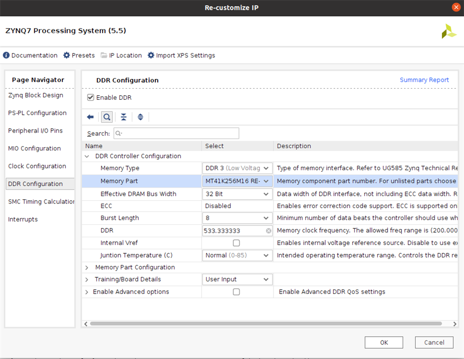
Processor Part number : XC7Z010-2CLG400I 

DDR3L Part number : MT41K256M16TW-107 AUT:P 

Case 1: we have configured DDR3L operating speed to 533.333MHz in Vivado and build the project same as Pico Zed board  ( Pico Zed board operating frequency is 533.333MHz)

Observation: only 3 lines were printed after that there is no progress after this lines 

U-Boot 2022.01-00194-gb31476685d (Sep 20 2022 - 06:35:33 +0000)

 CPU:   Zynq 7z010
Silicon: v3.1
DRAM:  ECC disabled 1 GiB

Case 2: configured the DDR3L operating frequency to 303MHz in Vivado 

Observation: Board is booted up and no errors found. 

We required to operate with 533.333MHz i request any suggestion can be helpful to resolve my issue. 

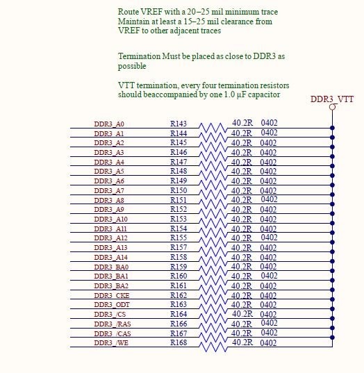
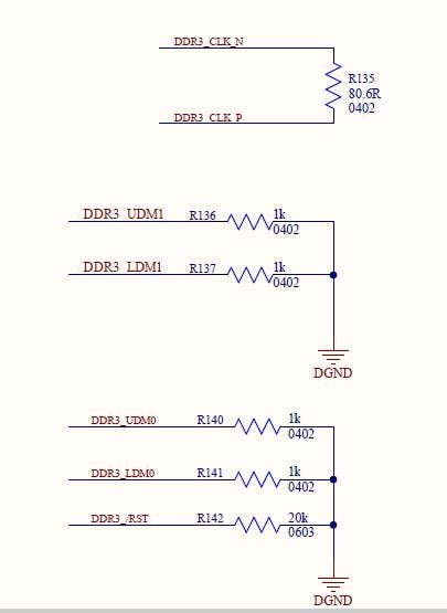
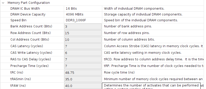
Let me know if we need to change the DDR timings. 

Thanks in advance  

  • Sign in to reply
  • Cancel

Top Replies

  • dyessgg
    dyessgg over 2 years ago +1
    Is this a custom board or a SOM? I'm assuming a custom board. 1. Have you correctly set the trace lengths for the DDR in Vivado? 2. Have you tested the DDR signal integrity? It really sounds like…
Parents
  • dyessgg
    dyessgg over 2 years ago

    Is this a custom board or a SOM?  I'm assuming a custom board.

    1. Have you correctly set the trace lengths for the DDR in Vivado?

    2. Have you tested the DDR signal integrity?

    It really sounds like you have a signal integrity issue.  Maybe termination not correct?

    • Cancel
    • Vote Up +1 Vote Down
    • Sign in to reply
    • Cancel
  • JANAKIRAM12137
    JANAKIRAM12137 over 2 years ago in reply to dyessgg

    Hi dyessgg ,

    please find the signal integrity waveforms for clock and data,

    Clock : Simulated with 800MHz

    image

    image

    Termination resistors we used for single ended was 40.2 Ohm and for Clock used 80.4 Ohm. 

    Termination Resistors

    image

    image

    Let me know if you need any more inputs. 

    Janakiram 

    • Cancel
    • Vote Up 0 Vote Down
    • Sign in to reply
    • Cancel
  • dyessgg
    dyessgg over 2 years ago in reply to JANAKIRAM12137

    These look WAY too clean for a real board.  The line "Clock : Simulated with 800MHz".  Is this actual captures from your board or some simulation?

    I'm not an expert, but the terminations look good to me.

    Are your trace lengths matched within tolerances?  Have you entered those trace lengths into Vivado to generate the startup configuration code?

    Are there discontinuities loo too many vias or crossing different ground planes?

    I recall a (long time ago) a board had weird DDR issues and it turned out the board was not being fed enough power.  A voltmeter could not capture the dips in voltage but a scope did.  Maybe check the power with a scope triggered at a very slight voltage drop.  Check all supplies related to the DDR.

    Beyond that, you're getting into the deep magic of DDR I tend to stay clear of.

    • Cancel
    • Vote Up 0 Vote Down
    • Sign in to reply
    • Cancel
Reply
  • dyessgg
    dyessgg over 2 years ago in reply to JANAKIRAM12137

    These look WAY too clean for a real board.  The line "Clock : Simulated with 800MHz".  Is this actual captures from your board or some simulation?

    I'm not an expert, but the terminations look good to me.

    Are your trace lengths matched within tolerances?  Have you entered those trace lengths into Vivado to generate the startup configuration code?

    Are there discontinuities loo too many vias or crossing different ground planes?

    I recall a (long time ago) a board had weird DDR issues and it turned out the board was not being fed enough power.  A voltmeter could not capture the dips in voltage but a scope did.  Maybe check the power with a scope triggered at a very slight voltage drop.  Check all supplies related to the DDR.

    Beyond that, you're getting into the deep magic of DDR I tend to stay clear of.

    • Cancel
    • Vote Up 0 Vote Down
    • Sign in to reply
    • Cancel
Children
  • sameeksh
    sameeksh over 2 years ago in reply to dyessgg

    Hi dyessgg ,

    Continuing with what JANAKIRAM12137 shared.
    We are using DDR3L MT41K256M16TW-107 AUT:P. The closet chip that is available on vivado is MT41K256M16 RE-125.
    [The Picozed board also has this same ddr IC and they used this exact configuration on vivado
    Our custom design is based on picozed eval board and it too has two DDR3L.]

    DDR controller configuation:- 
    Same as Picozed
    image

    Memory Part Configuration:-
    Kept it same as Picozed board.
    image

    Training Board details:-
    This details are filled based on the track lengths of our custom board (pls find the attached signals file that has the routing related values)
    image
    With this configuration values put in , I have seen the following observations:-
    1.At 303MHz : All the DDR tests are passing. The board boots up without any misbehavior.
    2.At 333MHz: The DDR test fails for 1024MB of data. The board booting is inconsistent
    3.At 400MHz: The DDR test fails for 256MB,512MB,1024MB. Board hardly boots
    4.At 533.3333333MHz : All the DDR tests fail.

    I have tried keeping the delay values exactly like the eval board, but again the behavior is same.

    Can you please share you insights based on these observations.

    Regards,
    Sameeksh Shetty

    • Cancel
    • Vote Up 0 Vote Down
    • Sign in to reply
    • Cancel
  • dyessgg
    dyessgg over 2 years ago in reply to sameeksh

    I don't see anything obviously wrong.  I would scope all of your power rails dealing with the DDR and trigger on any voltage dips.  

    It still sounds to me like a signal integrity issue.  You didn't answer the question about the eye diagrams being actual or simulated.  If simulated, make sure to capture real traces at the various frequency nodes you mentioned to see what is different.

    You're going beyond my experience now. 

    • Cancel
    • Vote Up 0 Vote Down
    • Sign in to reply
    • Cancel
  • JANAKIRAM12137
    JANAKIRAM12137 over 2 years ago in reply to dyessgg

    hi dyessgg above images was belongs to simulation. will provide the actual hardware waveforms and voltage dips observations as well. Thanks for your guidance. 

    Janakiram 

    • Cancel
    • Vote Up 0 Vote Down
    • Sign in to reply
    • Cancel
  • brianmckee
    brianmckee over 2 years ago in reply to JANAKIRAM12137

    If you can share the layout of the DDR3L it might help us deduce what needs to change.

    • Cancel
    • Vote Up 0 Vote Down
    • Sign in to reply
    • Cancel
  • JANAKIRAM12137
    JANAKIRAM12137 over 2 years ago in reply to brianmckee

    Hi i am not able to share the  PCB file but i can share my images, if my PC issues resolved i can upload the file by tomorrow.

    {gallery}My Gallery Title

    imageI

    ADDR_CMD_Routing Part 1

    image

    ADDR_CMD_Routing Part 2

    image

    Bank 0 Routing 

    image

    BANK 1 Routing

    image

    BANK 2 Routing

    image 

    BANK 3 Routing

    image 

    DDR3L  Placement 

    BANK 0 Routing lengths,

    Name Node Count Signal Length (mil) Total Pin/Package Length (mil) Routed Length (mil) Unrouted (Manhattan) (mil) Delay (ps) Margin
    L0_DQS_P_PP1 2 923.777 0 923.777 0 136.443 -4.581mil
    L0_DQS_N_PP1 2 928.358 0 928.358 0 137.243 Target
    L0_DDR3_D7_PP1 2 928.079 0 928.079 0 137.933 -0.279mil
    L0_DDR3_D6_PP1 2 925.902 0 925.902 0 137.498 -2.456mil
    L0_DDR3_D5_PP1 2 928.119 0 928.119 0 137.883 -0.239mil
    L0_DDR3_D4_PP1 2 925.07 0 925.07 0 137.405 -3.288mil
    L0_DDR3_D3_PP1 2 924.317 0 924.317 0 137.226 -4.041mil
    L0_DDR3_D2_PP1 2 924.083 0 924.083 0 137.185 -4.275mil
    L0_DDR3_D1_PP1 2 928.256 0 928.256 0 137.911 -0.102mil
    L0_DDR3_D0_PP1 2 924.308 0 924.308 0 137.22 -4.05mil
    DDR3_LDM0_PP1 2 925.749 0 925.749 0 137.473 -2.61mil

    BANK 1 Routing lengths,

    Name Node Count Signal Length (mil) Total Pin/Package Length (mil) Routed Length (mil) Unrouted (Manhattan) (mil) Delay (ps) Margin
    L1_DQS_P_PP1 2 700.443 0 700.443 0 99.758 -2.215mil
    L1_DQS_N_PP1 2 701.548 0 701.548 0 99.946 -1.109mil
    L1_DDR3_D15_PP1 2 701.858 0 701.858 0 100.551 -0.8mil
    L1_DDR3_D14_PP1 2 701.642 0 701.642 0 100.508 -1.016mil
    L1_DDR3_D13_PP1 2 701.636 0 701.636 0 100.502 -1.022mil
    L1_DDR3_D12_PP1 2 701.05 0 701.05 0 100.402 -1.608mil
    L1_DDR3_D11_PP1 2 702.249 0 702.249 0 100.617 -0.409mil
    L1_DDR3_D10_PP1 2 701.391 0 701.391 0 100.458 -1.267mil
    L1_DDR3_D9_PP1 2 701.906 0 701.906 0 100.559 -0.752mil
    L1_DDR3_D8_PP1 2 702.658 0 702.658 0 100.681 Target
    DDR3_UDM0_PP1 2 700.027 0 700.027 0 100.239 -2.631mil

    BANK 2 Routing lengths,

    Name Node Count Signal Length (mil) Total Pin/Package Length (mil) Routed Length (mil) Unrouted (Manhattan) (mil) Delay (ps) Margin
    L2_DQS_P_PP1 2 868.087 0 868.087 0 126.717 -0.547mil
    L2_DQS_N_PP1 2 868.098 0 868.098 0 126.719 -0.536mil
    L2_DDR3_D7_PP1 2 868.477 0 868.477 0 127.467 -0.157mil
    L2_DDR3_D6_PP1 2 868.609 0 868.609 0 127.49 -0.025mil
    L2_DDR3_D5_PP1 2 868.245 0 868.245 0 127.427 -0.388mil
    L2_DDR3_D4_PP1 2 868.106 0 868.106 0 127.403 -0.528mil
    L2_DDR3_D3_PP1 2 868.184 0 868.184 0 127.419 -0.449mil
    L2_DDR3_D2_PP1 2 868.634 0 868.634 0 127.494 Target
    L2_DDR3_D1_PP1 2 868.141 0 868.141 0 127.41 -0.492mil
    L2_DDR3_D0_PP1 2 868.517 0 868.517 0 127.477 -0.117mil
    DDR3_LDM1_PP1 2 868.146 0 868.146 0 127.409 -0.487mil

    BANK 3 Routing lengths,

    Name Node Count Signal Length (mil) Total Pin/Package Length (mil) Routed Length (mil) Unrouted (Manhattan) (mil) Delay (ps) Margin
    L3_DQS_P_PP1 2 754.838 0 754.838 0 109.021 -3.152mil
    L3_DQS_N_PP1 2 757.765 0 757.765 0 109.519 -0.225mil
    L3_DDR3_D15_PP1 2 756.425 0 756.425 0 109.829 -1.565mil
    L3_DDR3_D14_PP1 2 757.132 0 757.132 0 109.955 -0.858mil
    L3_DDR3_D13_PP1 2 755.739 0 755.739 0 109.713 -2.251mil
    L3_DDR3_D12_PP1 2 756.386 0 756.386 0 109.819 -1.604mil
    L3_DDR3_D11_PP1 2 757.99 0 757.99 0 110.096 Target
    L3_DDR3_D10_PP1 2 754.945 0 754.945 0 109.517 -3.046mil
    L3_DDR3_D9_PP1 2 757.862 0 757.862 0 110.073 -0.128mil
    L3_DDR3_D8_PP1 2 756.701 0 756.701 0 109.496 -1.289mil
    DDR3_UDM1_PP1 2 756.048 0 756.048 0 109.767 -1.943mil

    ADDR_CMD_CLK Routing Lengths,

    Name Node Count Signal Length (mil) Total Pin/Package Length (mil) Routed Length (mil) Unrouted (Manhattan) (mil) Delay (ps) Margin Name Node Count Signal Length (mil) Total Pin/Package Length (mil) Routed Length (mil) Unrouted (Manhattan) (mil) Delay (ps) Margin * Name Node Count Signal Length (mil) Total Pin/Package Length (mil) Routed Length (mil) Unrouted (Manhattan) (mil) Delay (ps) Margin
    ADD_CMD_U10_U11 Total
    DDR3_ODT_PP1 2 778.007 0.459 0 778.007 0 117.437 N/A DDR3_ODT_PP2 2 1996.951 0.92 0 1996.951 0 314.67 N/A 2774.958 2774.958 432.107
    DDR3_CLK_P_PP1 2 775.226 3.24 0 775.226 0 129.699 N/A DDR3_CLK_P_PP2 2 1997.871 0 0 1997.871 0 312.499 N/A 2773.097 2773.097 442.198
    DDR3_CLK_N_PP1 2 777.154 1.312 0 777.154 0 130.171 N/A DDR3_CLK_N_PP2 2 1994.903 2.968 0 1994.903 0 311.891 N/A 2772.057 2772.057 442.062
    DDR3_CKE_PP1 2 776.125 2.341 0 776.125 0 130.616 N/A DDR3_CKE_PP2 2 1997.01 0.861 0 1997.01 0 343.827 N/A 2773.135 2773.135 474.443
    DDR3_BA2_PP1 2 778.466 0 0 778.466 0 113.59 N/A DDR3_BA2_PP2 2 1996.528 1.343 0 1996.528 0 320.802 N/A 2774.994 2774.994 434.392
    DDR3_BA1_PP1 2 777.114 1.352 0 777.114 0 130.825 N/A DDR3_BA1_PP2 2 1997.321 0.55 0 1997.321 0 343.882 N/A 2774.435 2774.435 474.707
    DDR3_BA0_PP1 2 776.916 1.55 0 776.916 0 130.673 N/A DDR3_BA0_PP2 2 1994.704 3.167 0 1994.704 0 343.368 N/A 2771.62 2771.62 474.041
    DDR3_A14_PP1 2 775.849 2.617 0 775.849 0 111.405 N/A DDR3_A14_PP2 2 1997.334 0.537 0 1997.334 0 324.755 N/A 2773.183 2773.183 436.16
    DDR3_A13_PP1 2 776.13 2.336 0 776.13 0 130.655 N/A DDR3_A13_PP2 2 1995.41 2.461 0 1995.41 0 343.55 N/A 2771.54 2771.54 474.205
    DDR3_A12_PP1 2 777.661 0.805 0 777.661 0 111.719 N/A DDR3_A12_PP2 2 1995.854 2.017 0 1995.854 0 324.499 N/A 2773.515 2773.515 436.218
    DDR3_A11_PP1 2 776.774 1.692 0 776.774 0 111.564 N/A DDR3_A11_PP2 2 1994.285 3.586 0 1994.285 0 324.223 N/A 2771.059 2771.059 435.787
    DDR3_A10_PP1 2 777.199 1.267 0 777.199 0 117.324 N/A DDR3_A10_PP2 2 1994.861 3.01 0 1994.861 0 314.41 N/A 2772.06 2772.06 431.734
    DDR3_A9_PP1 2 778.126 0.34 0 778.126 0 130.998 N/A DDR3_A9_PP2 2 1994.081 3.79 0 1994.081 0 343.319 N/A 2772.207 2772.207 474.317
    DDR3_A8_PP1 2 778.267 0.199 0 778.267 0 117.584 N/A DDR3_A8_PP2 2 1996.304 1.567 0 1996.304 0 314.658 N/A 2774.571 2774.571 432.242
    DDR3_A7_PP1 2 777.33 1.136 0 777.33 0 130.864 N/A DDR3_A7_PP2 2 1996.531 1.34 0 1996.531 0 343.747 N/A 2773.861 2773.861 474.611
    DDR3_A6_PP1 2 776.664 1.802 0 776.664 0 117.304 N/A DDR3_A6_PP2 2 1995.268 2.603 0 1995.268 0 314.475 N/A 2771.932 2771.932 431.779
    DDR3_A5_PP1 2 776.864 1.602 0 776.864 0 130.782 N/A DDR3_A5_PP2 2 1994.281 3.59 0 1994.281 0 343.355 N/A 2771.145 2771.145 474.137
    DDR3_A4_PP1 2 777.114 1.352 0 777.114 0 117.414 N/A DDR3_A4_PP2 2 1994.589 3.282 0 1994.589 0 314.378 N/A 2771.703 2771.703 431.792
    DDR3_A3_PP1 2 775.432 3.034 0 775.432 0 113.198 N/A DDR3_A3_PP2 2 1996.079 1.792 0 1996.079 0 320.79 N/A 2771.511 2771.511 433.988
    DDR3_A2_PP1 2 776.167 2.299 0 776.167 0 117.276 N/A DDR3_A2_PP2 2 1996.034 1.837 0 1996.034 0 314.575 N/A 2772.201 2772.201 431.851
    DDR3_A1_PP1 2 776.565 1.901 0 776.565 0 130.729 N/A DDR3_A1_PP2 2 1994.389 3.482 0 1994.389 0 343.372 N/A 2770.954 2770.954 474.101
    DDR3_A0_PP1 2 776.683 1.783 0 776.683 0 117.327 N/A DDR3_A0_PP2 2 1996.444 1.427 0 1996.444 0 314.634 N/A 2773.127 2773.127 431.961
    DDR3_/WE_PP1 2 776.561 1.905 0 776.561 0 117.215 N/A DDR3_/WE_PP2 2 1996.321 1.55 0 1996.321 0 314.571 N/A 2772.882 2772.882 431.786
    DDR3_/RST_PP1 2 776.432 2.034 0 776.432 0 113.4 N/A DDR3_/RST_PP2 2 1995.601 2.27 0 1995.601 0 320.838 N/A 2772.033 2772.033 434.238
    DDR3_/RAS_PP1 2 775.784 2.682 0 775.784 0 111.391 N/A DDR3_/RAS_PP2 2 1994.908 2.963 0 1994.908 0 324.33 N/A 2770.692 2770.692 435.721
    DDR3_/CS_PP1 2 777.671 0.795 0 777.671 0 130.805 N/A DDR3_/CS_PP2 2 1997.392 0.479 0 1997.392 0 343.837 N/A 2775.063 2775.063 474.642
    DDR3_/CAS_PP1 2 776.371 2.095 0 776.371 0 117.346 N/A DDR3_/CAS_PP2 2 1996.661 1.21 0 1996.661 0 314.842 N/A 2773.032 2773.032 432.188

    Let me know if you need any more information.

    Thanks in advance. 

    Janakiram  

    • Cancel
    • Vote Up 0 Vote Down
    • Sign in to reply
    • Cancel
  • brianmckee
    brianmckee over 2 years ago in reply to JANAKIRAM12137

    A quick inspection looks like the data is correct, but double check the trace lengths and timings, just in case.

    Assuming the trace lengths are programmed properly into Vivado and the trace impedance and terminations are correct, the only thing I can think of is: have you regenerated your entire software stack with the new values generated by vivado. You can't use any firmware from the demo board.

    I personally haven't done this with Vivado yet, but with competitor tools, I had to generate a new u-boot and flash it onto the boot device to ensure that the timings were loaded properly on boot up before the DRAM training begins.

    Here's a dumb question, just in case: are you sure you have the right speed parts installed on the board? Double check that part number and speed grade.

    • Cancel
    • Vote Up 0 Vote Down
    • Sign in to reply
    • Cancel
  • JANAKIRAM12137
    JANAKIRAM12137 over 2 years ago in reply to brianmckee

    Hi brianmckee ,

    Thanks for the valuable inputs.

    we have cross checked the Trace lengths all are same as provided in the above, impedances we have maintained as suggested by the Xilinx for DDR3L ( 40Ohm and 80Ohm). 

    As per your suggestion we are going through the timings will update you soon. 

    Thanks for the support. 

    Janakiram 

    • Cancel
    • Vote Up 0 Vote Down
    • Sign in to reply
    • Cancel
  • brianmckee
    brianmckee over 2 years ago in reply to JANAKIRAM12137

    If you can't find any major mistakes in the data you entered into the tool, I can only think of little things to check, which shouldn't really affect 533 MHz.

    For example, the wiggles should use smooth curves, not angles and there should be a complete and solid ground under all traces to and from the DDR3.

    One other thing to try, check the dram timing provided by Xilinx in the tool against the specification for the exact 1066 DDR3 part you are using.

    Make sure the CAS latency and other timings are in bounds. Make sure you aren't using numbers that are too large because you are running half the clock rate of the DDR. I'm thinking about refresh and other timings that matter for volatile memory.

    If you still can't get it to run at speed, try delaying the critical timings by one clock just to see if you can get it to work. Then pull back the timings one at a time until it doesn't work. That will at least give you some idea what signal to look at with a scope.

    Also, check your termination resistors, is it possible they were populated with the wrong values?

    Have you looked at clock, ras, cas, we and a0 at the load to see what they look like? You need to check the eye pattern and make sure there isn't some errant ringing. Looking at the data eye patter should show no issue, unless there's a really bad impedance miscalculation.

    • Cancel
    • Vote Up 0 Vote Down
    • Sign in to reply
    • Cancel
element14 Community

element14 is the first online community specifically for engineers. Connect with your peers and get expert answers to your questions.

  • Members
  • Learn
  • Technologies
  • Challenges & Projects
  • Products
  • Store
  • About Us
  • Feedback & Support
  • FAQs
  • Terms of Use
  • Privacy Policy
  • Legal and Copyright Notices
  • Sitemap
  • Cookies

An Avnet Company © 2025 Premier Farnell Limited. All Rights Reserved.

Premier Farnell Ltd, registered in England and Wales (no 00876412), registered office: Farnell House, Forge Lane, Leeds LS12 2NE.

ICP 备案号 10220084.

Follow element14

  • X
  • Facebook
  • linkedin
  • YouTube