element14 Community
element14 Community
    Register Log In
  • Site
  • Search
  • Log In Register
  • About Us
  • Community Hub
    Community Hub
    • What's New on element14
    • Feedback and Support
    • Benefits of Membership
    • Personal Blogs
    • Members Area
    • Achievement Levels
  • Learn
    Learn
    • Ask an Expert
    • eBooks
    • element14 presents
    • Learning Center
    • Tech Spotlight
    • STEM Academy
    • Webinars, Training and Events
    • Learning Groups
  • Technologies
    Technologies
    • 3D Printing
    • FPGA
    • Industrial Automation
    • Internet of Things
    • Power & Energy
    • Sensors
    • Technology Groups
  • Challenges & Projects
    Challenges & Projects
    • Design Challenges
    • element14 presents Projects
    • Project14
    • Arduino Projects
    • Raspberry Pi Projects
    • Project Groups
  • Products
    Products
    • Arduino
    • Avnet Boards Community
    • Dev Tools
    • Manufacturers
    • Multicomp Pro
    • Product Groups
    • Raspberry Pi
    • RoadTests & Reviews
  • Store
    Store
    • Visit Your Store
    • Choose another store...
      • Europe
      •  Austria (German)
      •  Belgium (Dutch, French)
      •  Bulgaria (Bulgarian)
      •  Czech Republic (Czech)
      •  Denmark (Danish)
      •  Estonia (Estonian)
      •  Finland (Finnish)
      •  France (French)
      •  Germany (German)
      •  Hungary (Hungarian)
      •  Ireland
      •  Israel
      •  Italy (Italian)
      •  Latvia (Latvian)
      •  
      •  Lithuania (Lithuanian)
      •  Netherlands (Dutch)
      •  Norway (Norwegian)
      •  Poland (Polish)
      •  Portugal (Portuguese)
      •  Romania (Romanian)
      •  Russia (Russian)
      •  Slovakia (Slovak)
      •  Slovenia (Slovenian)
      •  Spain (Spanish)
      •  Sweden (Swedish)
      •  Switzerland(German, French)
      •  Turkey (Turkish)
      •  United Kingdom
      • Asia Pacific
      •  Australia
      •  China
      •  Hong Kong
      •  India
      •  Korea (Korean)
      •  Malaysia
      •  New Zealand
      •  Philippines
      •  Singapore
      •  Taiwan
      •  Thailand (Thai)
      • Americas
      •  Brazil (Portuguese)
      •  Canada
      •  Mexico (Spanish)
      •  United States
      Can't find the country/region you're looking for? Visit our export site or find a local distributor.
  • Translate
  • Profile
  • Settings
Dev Tools
  • Products
  • More
Dev Tools
Forum Digitally Controlled Variable Load
  • Forum
  • Documents
  • Files
  • Members
  • Mentions
  • Sub-Groups
  • Tags
  • More
  • Cancel
  • New
Join Dev Tools to participate - click to join for free!
Actions
  • Share
  • More
  • Cancel
Forum Thread Details
  • State Verified Answer
  • Replies 8 replies
  • Answers 4 answers
  • Subscribers 77 subscribers
  • Views 892 views
  • Users 0 members are here
  • mosfets
  • mosfet_drivers
Related

Digitally Controlled Variable Load

Former Member
Former Member over 8 years ago

Morning all,


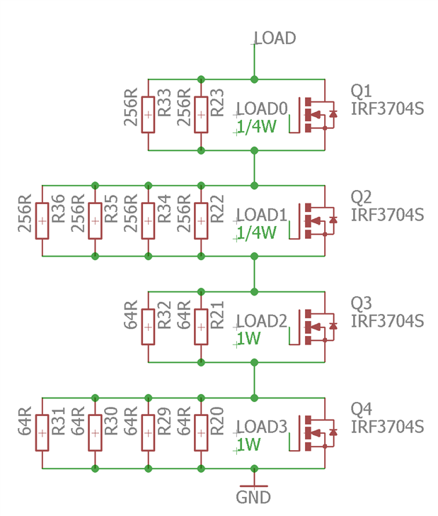
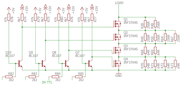
Query regarding shunting series resistors with MOSFETs to create a high power load...


System:

Up to a 10V source, capable of up to 5A peak, well under 1A continuous.  Source voltage decreases with time down to zero, I want to get as close to zero as possible without the resistance changing (i.e. the MOSFET changing state due to low gate voltage).


Requirement:

To be able to place a variable load across the source which is digitally controlled, ideally with MOSFETs not relays.


Question:

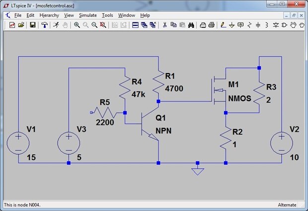
Most MOSFET drivers use a charge pump which is driven from the high side.  My high side changes, however.  Is there a way I can drive the MOSFET driver with a separate power source?


image

  • Sign in to reply
  • Cancel
Parents
  • michaelkellett
    0 michaelkellett over 8 years ago

    I can't quite reconcile your spec with the schematic.

    What is the maximum voltage that will be applied at the point marked "LOAD" relative to GND ?

    Will the applied voltage always be positive.


    How fast must the MOSFETs switch on and off and how fast might the applied voltage at "LOAD" change.


    The MOSFET you have chosen will cope with a gate voltage ref. source of +/- 20V max.

    If, as I guess, the maximum applied voltage at "LOAD"  will only be 10V you can drive the MOSFETs with gate voltages of 15V and ensure that the topmost MOSFET will be well and truly on (13.5mR at 12A from the data sheet). If you don't need to switch fast you can use CMOS logic, open collector/drain transistor drivers with pull up resistors or op amps to drive the MOSFETs. The clever feature of MOSFET driver chips is that they can source and sink large currents but you only need this if you must switch the MOSFET on and off quickly or if there are very fast changes in drain voltage.


    MK

    • Cancel
    • Vote Up 0 Vote Down
    • Sign in to reply
    • Verify Answer
    • Reject Answer
    • Cancel
  • Former Member
    0 Former Member over 8 years ago in reply to michaelkellett

    Hi Michael


    The voltage at LOAD is 0-10V, won't go negative.  It is a supercapacitor if that helps!


    The MOSFET doesn't need to switch fast at all, tens of milliseconds is fine.


    So in essence I could have a separate power supply (I already have 5V on the PCB), boost this to 15V, and use a P-Ch MOSFET to drive each of the N-Ch MOSFET gates?  From all the drivers I have found, they rely upon the drain voltage being the IC VCC and cut out at a nominal voltage, e.g. 2V7.  I the MOSFET to be on all the way down to a zero Drain-Source voltage.


    Does the above sound sensible?


    Thanks

    • Cancel
    • Vote Up 0 Vote Down
    • Sign in to reply
    • Verify Answer
    • Cancel
  • michaelkellett
    0 michaelkellett over 8 years ago in reply to Former Member

    Something like this would do:


    image


    V2 is your supercap voltage, M1 is one of your MOSFETs, R2 limits the lowest load resistance you use.

    Apply the control voltage to the free end of R5, if you are using 5V logic this will work fine. If 3.3V logic then V3 needs to be 3.3V.

    If the micro starts up (I'm assuming this is controlled by a micro) with the drive to R5 open circuit then R4 turns on Q1 and makes sure that the MOSFET is off.

    Q1 needs a gain of at least 100 at Ic = 3mA.

    The MOSFET will be on if Q1 is off (input low) - V2 won't affect this (so long as it's less than 10V).


    You can have several MOSFETs in series each one will need its own drive transistor and associated resistors.


    MK

    • Cancel
    • Vote Up 0 Vote Down
    • Sign in to reply
    • Verify Answer
    • Reject Answer
    • Cancel
  • Former Member
    0 Former Member over 8 years ago in reply to michaelkellett

    Like this?


    Two questions:

    1. I get how Q4 will work, but how about the high side MOSFETs?  Will they not be permanently off as the gate-source voltage may be low/negative? e.g. if Q4 is on then the source voltage at Q3 would be pulled to 10V?

    2. You have V1 on your schematic as 15V.  Not sure where this has come from?  I am assuming this is a boost converter to solve the problem above?  In which case is this just a deconstructed high side MOSFET driver with the charge pump being powered from the Vlogic side rather than Vout?


    image


    Many thanks


    Simon

    • Cancel
    • Vote Up 0 Vote Down
    • Sign in to reply
    • Verify Answer
    • Cancel
  • michaelkellett
    0 michaelkellett over 8 years ago in reply to Former Member

    If LOAD = 10V and all MOSFETs all off the voltage on Q1 source and Q2 drain =  10/(128 + 64 + 32 + 16)*(64 + 32 + 16) = 4.66V, if you now turn Q10 off the gate of Q1 will change form about 0.1V to 15V and Q1 will turn on.


    By using 15V for the gate drive positive voltage we can be sure that with a maximum of 10V on LOAD we never have less than 5V positive gate drive to turn a MOSFET on and that the off voltage (ref the MOSFETs source) will be between 0.1 and -10V.


    I'm not sure why you think Q4 on could result in Q3 source at 10V, if Q4 is on it will connect its drain and Q3 source to GND = 0V


    V1  = 15V is a DC supply that you must make somehow. It must be there all the time, independently of the load voltage. You could use a MOSFET drive if you pick one with a separate input pin for the high drive voltage - doing it with discrete parts makes it  more obvious what is going on.


    You really should have  a resistor in series with Q4 source and GND, otherwise if you accidentally turn all the MOSFETs on you will get  a very large current which may damage things.


    I'm assuming that you know that there is a much more commonly used way to achieve the variable load current by using a DAC, an op amp, 1 MOSFET and a sense resistor.


    MK

    • Cancel
    • Vote Up 0 Vote Down
    • Sign in to reply
    • Verify Answer
    • Reject Answer
    • Cancel
  • Former Member
    0 Former Member over 8 years ago in reply to michaelkellett

    Hi MK, again, thanks very much for replying.


    Yep, aware of the opamp route but it is a constant resistance I need, not constant current.  We'll be testing the supercap at different resistance loads (among other things).


    I'm not sure about the Q3/4 statement I made (it was late last night), sorry lol.  Please ignore!


    Thanks for the current spike point.  I have a few upstream components adding a bit of resistance but one has a peak load of 6A.  I have added a 1R6 resistor for now which reduces the spike to 5.9A.  I'll revisit this later and consider the dissipation as  that's going to be rather high.


    So taking the point about needing a separate 15V supply, and since the IRF3704 has a gate tolerant of +-20V, would this not be simpler with lower component count (space is a premium rather than cost) or am I missing something...


    image


    Cheers

    Simon

    • Cancel
    • Vote Up 0 Vote Down
    • Sign in to reply
    • Reject Answer
    • Cancel
  • michaelkellett
    0 michaelkellett over 8 years ago in reply to Former Member

    Using little MOSFETs as drivers is fine.

    BSS101 is obsolete with many people so I didn't find a  data sheet, 2N7000 would do fine.

    Is it really TTL levels (0.4 -> 2.6) or CMOS logic on 5V supply giving 0 -> 5V - probably doesn't matter but I didn't think anyone used TTL any more image


    MK

    • Cancel
    • Vote Up 0 Vote Down
    • Sign in to reply
    • Verify Answer
    • Reject Answer
    • Cancel
  • Former Member
    0 Former Member over 8 years ago in reply to michaelkellett

    It's CMOS, I'm still stuck in the past with my terminology!  Coming from an I2C GPIO expander at 5V.


    Thanks for all your help.

    • Cancel
    • Vote Up 0 Vote Down
    • Sign in to reply
    • Verify Answer
    • Cancel
Reply
  • Former Member
    0 Former Member over 8 years ago in reply to michaelkellett

    It's CMOS, I'm still stuck in the past with my terminology!  Coming from an I2C GPIO expander at 5V.


    Thanks for all your help.

    • Cancel
    • Vote Up 0 Vote Down
    • Sign in to reply
    • Verify Answer
    • Cancel
Children
No Data
element14 Community

element14 is the first online community specifically for engineers. Connect with your peers and get expert answers to your questions.

  • Members
  • Learn
  • Technologies
  • Challenges & Projects
  • Products
  • Store
  • About Us
  • Feedback & Support
  • FAQs
  • Terms of Use
  • Privacy Policy
  • Legal and Copyright Notices
  • Sitemap
  • Cookies

An Avnet Company © 2025 Premier Farnell Limited. All Rights Reserved.

Premier Farnell Ltd, registered in England and Wales (no 00876412), registered office: Farnell House, Forge Lane, Leeds LS12 2NE.

ICP 备案号 10220084.

Follow element14

  • X
  • Facebook
  • linkedin
  • YouTube