element14 Community
element14 Community
    Register Log In
  • Site
  • Search
  • Log In Register
  • About Us
  • Community Hub
    Community Hub
    • What's New on element14
    • Feedback and Support
    • Benefits of Membership
    • Personal Blogs
    • Members Area
    • Achievement Levels
  • Learn
    Learn
    • Ask an Expert
    • eBooks
    • element14 presents
    • Learning Center
    • Tech Spotlight
    • STEM Academy
    • Webinars, Training and Events
    • Learning Groups
  • Technologies
    Technologies
    • 3D Printing
    • FPGA
    • Industrial Automation
    • Internet of Things
    • Power & Energy
    • Sensors
    • Technology Groups
  • Challenges & Projects
    Challenges & Projects
    • Design Challenges
    • element14 presents Projects
    • Project14
    • Arduino Projects
    • Raspberry Pi Projects
    • Project Groups
  • Products
    Products
    • Arduino
    • Avnet Boards Community
    • Dev Tools
    • Manufacturers
    • Multicomp Pro
    • Product Groups
    • Raspberry Pi
    • RoadTests & Reviews
  • Store
    Store
    • Visit Your Store
    • Choose another store...
      • Europe
      •  Austria (German)
      •  Belgium (Dutch, French)
      •  Bulgaria (Bulgarian)
      •  Czech Republic (Czech)
      •  Denmark (Danish)
      •  Estonia (Estonian)
      •  Finland (Finnish)
      •  France (French)
      •  Germany (German)
      •  Hungary (Hungarian)
      •  Ireland
      •  Israel
      •  Italy (Italian)
      •  Latvia (Latvian)
      •  
      •  Lithuania (Lithuanian)
      •  Netherlands (Dutch)
      •  Norway (Norwegian)
      •  Poland (Polish)
      •  Portugal (Portuguese)
      •  Romania (Romanian)
      •  Russia (Russian)
      •  Slovakia (Slovak)
      •  Slovenia (Slovenian)
      •  Spain (Spanish)
      •  Sweden (Swedish)
      •  Switzerland(German, French)
      •  Turkey (Turkish)
      •  United Kingdom
      • Asia Pacific
      •  Australia
      •  China
      •  Hong Kong
      •  India
      •  Korea (Korean)
      •  Malaysia
      •  New Zealand
      •  Philippines
      •  Singapore
      •  Taiwan
      •  Thailand (Thai)
      • Americas
      •  Brazil (Portuguese)
      •  Canada
      •  Mexico (Spanish)
      •  United States
      Can't find the country/region you're looking for? Visit our export site or find a local distributor.
  • Translate
  • Profile
  • Settings
Dev Tools
  • Products
  • More
Dev Tools
Forum Design of PCB Trace Routing
  • Forum
  • Documents
  • Files
  • Members
  • Mentions
  • Sub-Groups
  • Tags
  • More
  • Cancel
  • New
Join Dev Tools to participate - click to join for free!
Actions
  • Share
  • More
  • Cancel
Forum Thread Details
  • Replies 12 replies
  • Subscribers 78 subscribers
  • Views 2100 views
  • Users 0 members are here
  • pcb layout
  • pcb board design
  • design pcb
Related

Design of PCB Trace Routing

perigalacticon
perigalacticon over 7 years ago

Looking for advice for designing a PCB with several functions.  I am an amateur PCB designer and only designed one other small board but it worked.


This project currently has the following features:


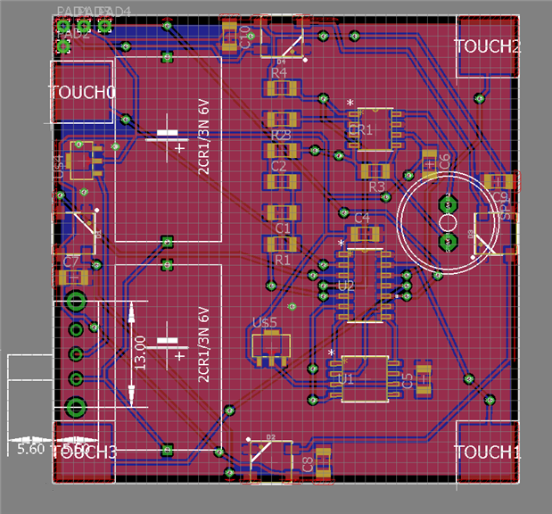
1.  5V & 3.3V power regulators.

2.  SPI signals from an ATTINY841-SU SOIC-14 MCU to a Dataflash SPI flash soic-8 IC.

3.  1W audio amplifier to external 8R .5W speaker.

4.  5x WS2812B surface mount Leds.

5.  5X capacitive touch pads (externally connected).

6 2x 6V  2CR1/3N2CR1/3N batteries in parallel

7.  2.25" square PCB, 2-sided, standard options.


I am looking for advice as to how to route the traces for best performance, I'm working with Eagle 8.3.2.  This a project for some gifts I am making for Halloween in a quantity of ~50.


I am mainly concerned about signal integrity and noise, especially the capacitive touch connections.  Currently I routed these last but there are many vias on these traces and I'm concerned that nearby external objects may affect the capacitance readings.  I could route these first on top with no vias but then the other signal traces are more complicated.  Is SPI sensitive to routing with several vias?  How about WS2812B data signals or small voltage audio signals?  How sensitive should I expect this system to be to routing overall?

  • Sign in to reply
  • Cancel

Top Replies

  • michaelkellett
    michaelkellett over 7 years ago +1
    Why not post a.pdf of where you are at the moment - much easier to understand. Don't use traces as thin as 0.005" (0.125mm) unless you reall need to go that thin (which I doubt). You'll get cheaper and…
  • michaelkellett
    michaelkellett over 7 years ago in reply to perigalacticon +1
    Hello Stephen, Any capacitance to ground will reduce the sensitivity of your touch system - if you are using a standard library and method defined by Atmel/Microchip for the ATiny then it will have supporting…
  • michaelkellett
    michaelkellett over 7 years ago in reply to perigalacticon +1
    I just looked again at your batteries: Check the data here: https://www.duracell.com/en-us/techlibrary/product-technical-data-sheets?region=262&code=px28l This battery (and the Duracells will be better…
  • saravananeceait
    saravananeceait over 7 years ago

    SPI signals from an ATTINY841-SU SOIC-14 MCU to a Dataflash SPI flash soic-8 IC : You can go with 5.00 Mils trace width

    5x WS2812B surface mount Leds : You can go with 5.00 Mils trace width

    I am sure about these two you can route 5 mils!

    If its  correct let me know or else suggest i'll learn something!


    • Cancel
    • Vote Up 0 Vote Down
    • Sign in to reply
    • Cancel
  • michaelkellett
    michaelkellett over 7 years ago

    Why not post  a.pdf of where you are at the moment - much easier to understand.

    Don't use traces as thin as 0.005" (0.125mm) unless you reall need to go that thin (which I doubt). You'll get cheaper and more reliable boards if you use more relaxed design rules (with your parts I would try for 0.25mm track and gap to start with). Power traces should be wider, according to current.


    SPI from the ATTINY and connections to the WS2812B will stand a reasonable amount of vias, crossovers etc.


    You will do well to keep the tracks for the touch switches away from other tracks, especially ones with switching signals.

    Keep the audio signals away from the high speed switching signals.


    MK

    • Cancel
    • Vote Up +1 Vote Down
    • Sign in to reply
    • Cancel
  • perigalacticon
    perigalacticon over 7 years ago in reply to michaelkellett

    Ok, here we are, I couldn't export a pdf though:  There are vias on every signal I believe.  I haven't studied PCB design, but this board should be simple by most standards.  The speaker outline on the right is not used for mounting it's just to run the wires to it.  My approach was to run power first, keeping separate supplies to the major systems.  The WS2812s will draw the most current, I put them on their own 5V supply branch.  I am considering re-routing putting the cap-touch traces on top as a priority with no vias so they can't be influenced by objects near the bottom of the board enclosure.


    image

    • Cancel
    • Vote Up 0 Vote Down
    • Sign in to reply
    • Cancel
  • michaelkellett
    michaelkellett over 7 years ago in reply to perigalacticon

    The best way to do this board would be to put the ground pour and all non-touch traces on one side and the touch traces and pad on the other. Remove the ground pour under the touch pads, it won't hurt under the traces. You probably couldn't route it like that but you might get very close.


    If you just want to tweak what you have now, then increase the gap between the ground pour and the touch traces, remove the ground pour under the touch pads.


    You could put U1 closer to U2 to shorten the SPI traces but they should be fine as they are. It might be good to get the pads in the top left corner further from the touch pad, same with the connector.


    If you want to post a schematic we can comment on that too !


    MK

    • Cancel
    • Vote Up 0 Vote Down
    • Sign in to reply
    • Cancel
  • perigalacticon
    perigalacticon over 7 years ago in reply to michaelkellett

    Thanks for your suggestions.  This is my first project with Eagle.  I am actually going to attach copper conductive adhesive tape to the touch pads, and the tape will attach to the externally mounted touch surfaces.  This device is just meant to be low cost and last a few weeks.  As far as the part spacing I was trying to keep it reasonably spaced to make assembly easier as I am doing it myself, thus the 1206 parts as well.


    Some more questions:


    1.  As the touch pads on the PCB are actually connection points for the tape do you still recommend removing the ground plane there?


    2.  Can you tell me what is printed on the silkscreen from the Eagle layers ?  I have a lot of text showing on the board from different sources but I just want the component names and outlines on the silkscreen layer like any normal board.  How do I set up the silkscreen like this?


    The schematic is large I need some time to figure out how to post it so you can see it.

    • Cancel
    • Vote Up 0 Vote Down
    • Sign in to reply
    • Cancel
  • michaelkellett
    michaelkellett over 7 years ago in reply to perigalacticon

    Hello Stephen,


    Any capacitance to ground will reduce the sensitivity of your touch system - if you are using a standard library and method defined by Atmel/Microchip for the ATiny then it will have supporting documentation and advice.


    I can't help you with Eagle because I don't use it.


    I find no problem with hand soldering 0603 parts, and I can do 0402 at a pinch but that isn't so much fun.


    If you are hand soldering a surface mount board there is very little penalty in placing components on both sides, so you could easily make this board half the size if you wanted to (batteries, speaker and touch connections on one side and everything else on the other).


    MK

    • Cancel
    • Vote Up +1 Vote Down
    • Sign in to reply
    • Cancel
  • michaelkellett
    michaelkellett over 7 years ago in reply to perigalacticon

    I just looked again at your batteries:


    Check the data here:


    https://www.duracell.com/en-us/techlibrary/product-technical-data-sheets?region=262&code=px28l


    This battery (and the Duracells will be better than most) offers most of its life at 5.2V or less - two in parallel to power your design doesn't seem right since you have a 5V regulator.


    MK

    • Cancel
    • Vote Up +1 Vote Down
    • Sign in to reply
    • Cancel
  • perigalacticon
    perigalacticon over 7 years ago in reply to michaelkellett

    Thanks, the batteries I received measure at 6.2V.  I think they may be a different chemistry because they can supply 80mA each and up to 250 peak.  Voltage quickly drops with current but I didn't want to risk hurting anything.  I will consider removing it after I test some prototypes.  I rerouted the board to keep the cap touch on the top layer with no vias and removed the ground plane from under the touch pads, but I have to confirm this is the right strategy because I am using a simple ADC based touch measurement that just utilizes the ADC internal capacitance to measure external capacitance.  I was wondering if you have ever made a device with a spiflash memory because I have a problem which is if I leave the chip connected to the MCU by SPI then if I program the MCU the data on the spiflash is getting erased, even though the spiflash write-protect pin is asserted.

    image

    • Cancel
    • Vote Up +1 Vote Down
    • Sign in to reply
    • Cancel
  • perigalacticon
    perigalacticon over 7 years ago in reply to perigalacticon

    Thanks for the suggestion for mounting parts on the bottom but it's designed to fit nicely in an enclosure of this size for now.  I will solder them using an oven, stencil and solder paste.

    • Cancel
    • Vote Up +1 Vote Down
    • Sign in to reply
    • Cancel
  • michaelkellett
    michaelkellett over 7 years ago in reply to perigalacticon

    I've used lots of SPi flash chips and never had the problem you describe (I've had plenty of different problems of course image. I'd need to see a schematic to make some suggestions as to the mystery erasing. (and might need to see the code as well.)


    MK

    • Cancel
    • Vote Up +1 Vote Down
    • Sign in to reply
    • Cancel
>
element14 Community

element14 is the first online community specifically for engineers. Connect with your peers and get expert answers to your questions.

  • Members
  • Learn
  • Technologies
  • Challenges & Projects
  • Products
  • Store
  • About Us
  • Feedback & Support
  • FAQs
  • Terms of Use
  • Privacy Policy
  • Legal and Copyright Notices
  • Sitemap
  • Cookies

An Avnet Company © 2025 Premier Farnell Limited. All Rights Reserved.

Premier Farnell Ltd, registered in England and Wales (no 00876412), registered office: Farnell House, Forge Lane, Leeds LS12 2NE.

ICP 备案号 10220084.

Follow element14

  • X
  • Facebook
  • linkedin
  • YouTube