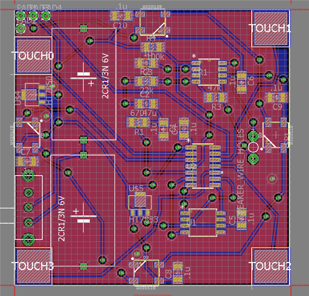
Looking for advice for designing a PCB with several functions. I am an amateur PCB designer and only designed one other small board but it worked.
This project currently has the following features:
1. 5V & 3.3V power regulators.
2. SPI signals from an ATTINY841-SU SOIC-14 MCU to a Dataflash SPI flash soic-8 IC.
3. 1W audio amplifier to external 8R .5W speaker.
4. 5x WS2812B surface mount Leds.
5. 5X capacitive touch pads (externally connected).
6 2x 6V 2CR1/3N2CR1/3N batteries in parallel
7. 2.25" square PCB, 2-sided, standard options.
I am looking for advice as to how to route the traces for best performance, I'm working with Eagle 8.3.2. This a project for some gifts I am making for Halloween in a quantity of ~50.
I am mainly concerned about signal integrity and noise, especially the capacitive touch connections. Currently I routed these last but there are many vias on these traces and I'm concerned that nearby external objects may affect the capacitance readings. I could route these first on top with no vias but then the other signal traces are more complicated. Is SPI sensitive to routing with several vias? How about WS2812B data signals or small voltage audio signals? How sensitive should I expect this system to be to routing overall?


