


Hello!
I wanted to take a moment to cross post a blog article by one of our lead applications experts, Ganesh Raaja. We will continue to post Ganesh's blog posts to the community as they are written. The link to his post can be found here:
http://www.cypress.com/?rID=93033&cache=0
I have also posted his article in the text below.
I hope this example can help you in your design.
Best,
Matt
Measuring VDD (Battery Volts) in PSoC 4 – Author Ganesh Raaja
Usually in battery operated applications, the microcontroller also measures the level of the battery and either displays the percentage of the battery left or generates an alarm when the battery level is getting low. There are two methods to measure battery voltage.
Method #1: In microcontrollers that have an internal ADC reference, the straightforward approach is to use a potential divider and scale down VDD to the ADC s measurement range. For example, if the internal VREF of the ADC is 1.024V, and we need to measure VDD which can vary from 3.0V to 4.2V (this is the range of a Lithium Ion battery), the following circuit may be used.
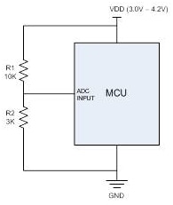
In the above circuit, R1 and R2 form a potential divider and would develop 1.024V when VDD equals 4.43V. So, for a 12 bit ADC, VDD may be measured by the following equation.
VDD = (4.43/4095) * ADC Counts
Method #2: In microcontrollers that do not have an internal ADC reference, but use VDD as the reference, we need an external reference to measure VDD.

In the above circuit, an external reference of 1.2V is connected to the ADC input. As the reference of the ADC is VDD, the ADC counts for VDD would always be 4095 counts. So, the ADC counts while measuring the external reference would be proportional to VDD. For a 12 bit ADC, VDD can now be calculated using following formula.
VDD = (1.2V * 4095) / ADC Counts
Both the above methods have a disadvantage that they require external components. We can implement the same VDD measurement in PSoC4 without using any external components. Let us see how.
PSoC4 Implementation
The diagram below shows the block diagram of the ADC inside PSoC4.

The input to the SAR ADC can be directly from the SARMUX in Port2 or from the AMUXBUS that can connect any pin to the ADC. The SARREF block generates the reference to the ADC. Below picture shows the SARREF block.

The reference to the ADC can be one of three voltages 1.024V, VDD or VDD/2. There is a bypass switch that brings out the output of the reference buffer to P1.7. The intent of this bypass switch is to reduce noise on the VREF by connecting an external bypass capacitor. We are going to use this bypass switch and Method #2 described earlier to measure VDD.
Following are the steps to measure VDD:
Connect an external bypass capacitor 1uF to P1[7].
Set the reference of ADC to VREF and enable the bypass switch. Keep the bypass enabled for a short time, say 25ms. This charges the 1uF capacitor to 1.024V.
Disable the bypass switch. Now the capacitor holds the 1.024V (like a sample and hold circuit)
Change the reference of the ADC to VDD, connect P1[7] as input to the ADC and measure the voltage.
VDD can then be calculated using the formula:
VDD = (1.024 * 2047) / ADC Counts P1[7]
The SAR ADC in PSoC4 is 12 bits. Then why am I using 2047 and not 4095 in the above equation? With the ADC configured for single ended measurement, the effective resolution of the ADC becomes 11 bits and hence the full scale count of 2047.
Let us now take a look at the project. Figure below shows the schematic of the project.

Place an OpAmp configured as a buffer. Place an analog input pin and connect this pin to the input of the buffer. Assign P1[7] to this pin. Place an ADC and configure the ADC for a reference of VDDA (we will dynamically change this in code). Select the Single Ended Negative Input to VSSA.
Following firmware will now take care of the VDD measurement. The result is availabe in the variable "Vdd" in millivolts.
void main()
{
int16 Vref;
int16 Vdd;
uint32 SARControlReg;
/* Start the LCD, OpAmp and ADC */
OpAmp_Buffer_Start();
ADC_Start();
for(;;)
{
/* Set the reference to VBG and enable reference bypass */
SARControlReg = CY_GET_REG32(CYREG_SAR_CTRL);
SARControlReg &= ~0x000000F0;
SARControlReg |= 0x000000C0;
CY_SET_REG32(CYREG_SAR_CTRL, SARControlReg);
/* 25ms delay for reference capacitor to charge */
CyDelay(25);
/* Set the reference to VDD and disable reference bypass */
SARControlReg = CY_GET_REG32(CYREG_SAR_CTRL);
SARControlReg &= ~0x000000F0;
SARControlReg |= 0x00000070;
CY_SET_REG32(CYREG_SAR_CTRL, SARControlReg);
/* Perform an ADC conversion */
ADC_StartConvert();
ADC_IsEndConversion(ADC_WAIT_FOR_RESULT);
Vref = ADC_GetResult16(0x00);
/* Calculate Vdd */
Vdd = (1024*2047)/Vref;
}
}