element14 Community
element14 Community
    Register Log In
  • Site
  • Search
  • Log In Register
  • Community Hub
    Community Hub
    • What's New on element14
    • Feedback and Support
    • Benefits of Membership
    • Personal Blogs
    • Members Area
    • Achievement Levels
  • Learn
    Learn
    • Ask an Expert
    • eBooks
    • element14 presents
    • Learning Center
    • Tech Spotlight
    • STEM Academy
    • Webinars, Training and Events
    • Learning Groups
  • Technologies
    Technologies
    • 3D Printing
    • FPGA
    • Industrial Automation
    • Internet of Things
    • Power & Energy
    • Sensors
    • Technology Groups
  • Challenges & Projects
    Challenges & Projects
    • Design Challenges
    • element14 presents Projects
    • Project14
    • Arduino Projects
    • Raspberry Pi Projects
    • Project Groups
  • Products
    Products
    • Arduino
    • Avnet Boards Community
    • Dev Tools
    • Manufacturers
    • Multicomp Pro
    • Product Groups
    • Raspberry Pi
    • RoadTests & Reviews
  • About Us
  • Store
    Store
    • Visit Your Store
    • Choose another store...
      • Europe
      •  Austria (German)
      •  Belgium (Dutch, French)
      •  Bulgaria (Bulgarian)
      •  Czech Republic (Czech)
      •  Denmark (Danish)
      •  Estonia (Estonian)
      •  Finland (Finnish)
      •  France (French)
      •  Germany (German)
      •  Hungary (Hungarian)
      •  Ireland
      •  Israel
      •  Italy (Italian)
      •  Latvia (Latvian)
      •  
      •  Lithuania (Lithuanian)
      •  Netherlands (Dutch)
      •  Norway (Norwegian)
      •  Poland (Polish)
      •  Portugal (Portuguese)
      •  Romania (Romanian)
      •  Russia (Russian)
      •  Slovakia (Slovak)
      •  Slovenia (Slovenian)
      •  Spain (Spanish)
      •  Sweden (Swedish)
      •  Switzerland(German, French)
      •  Turkey (Turkish)
      •  United Kingdom
      • Asia Pacific
      •  Australia
      •  China
      •  Hong Kong
      •  India
      •  Korea (Korean)
      •  Malaysia
      •  New Zealand
      •  Philippines
      •  Singapore
      •  Taiwan
      •  Thailand (Thai)
      • Americas
      •  Brazil (Portuguese)
      •  Canada
      •  Mexico (Spanish)
      •  United States
      Can't find the country/region you're looking for? Visit our export site or find a local distributor.
  • Translate
  • Profile
  • Settings
BeagleBoard
  • Products
  • Dev Tools
  • Single-Board Computers
  • BeagleBoard
  • More
  • Cancel
BeagleBoard
Blog BBB - High speed data acquisition and web-based UI
  • Blog
  • Forum
  • Documents
  • Quiz
  • Polls
  • Files
  • Members
  • Mentions
  • Sub-Groups
  • Tags
  • More
  • Cancel
  • New
Join BeagleBoard to participate - click to join for free!
  • Share
  • More
  • Cancel
Group Actions
  • Group RSS
  • More
  • Cancel
Engagement
  • Author Author: shabaz
  • Date Created: 4 Aug 2013 1:17 AM Date Created
  • Views 11499 views
  • Likes 7 likes
  • Comments 93 comments
  • test
  • beaglebone_black
  • bbb
  • texas_intruments
  • measurement
  • bb_black
  • beagle_bone_black
Related
Recommended

BBB - High speed data acquisition and web-based UI

shabaz
shabaz
4 Aug 2013

Introduction

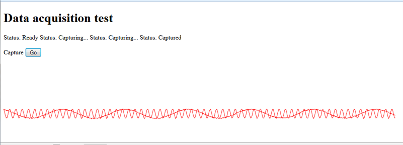
This was a fun yet initially challenging experiment, to find a convenient way to read in data at a reasonably high speed on a BeagleBone Black. This photo shows the results from a mobile, showing a couple of sampled waveforms (100kHz and 1MHz sinewaves in this case).

image

This was another capture of the same signals on a PC (this is an older picture with a x10 probe so the amplitude is a little low in the photo - it should fill the screen).

image


What does it do?

In its current state, it grabs analog data from an ADC, and dumps it into memory on the BBB, ready to be displayed or further processed. It could be used for gathering analog information from sensors, CCDs or other data acquisition use-cases. To be reasonably useful, the desire was for it to support 20Mbytes/sec of data or more. It does achieve this, but it is for further study to find higher speed methods.


How does it work?

A few different ways were considered. The initial approach was using an FTDI device (USB interface). However the method described here just feeds data directly into the on-chip 200MHz PRU that is part of the Beaglebone’s AM3359 chip. Other methods are possible too.

It was also desired to have an external clock, so that the data could be sampled at a determinable jitter, so that it could be useful for frequency analysis, or maybe Software Defined Radio (SDR).                                                           

The overall approach that was taken is outlined here.                                                                                                                                                                                  

image

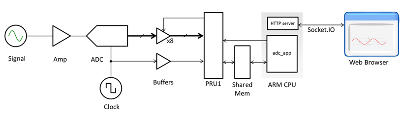
The analog signal was amplified and fed into a high-speed ADC (A parallel bus ADC is needed in order to achieve high throughput).

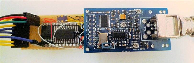
A pre-built amp+ADC board was used from KNJN (note: in my opinion it is not a good choice, because it is closed source; there are no circuit diagrams for it so it is hard to modify it, the datasheet is sparse and also it is expensive; better to construct one up manually).

A linux application (called adc_app in the diagram) was used to kick off the PRU code which reads in data and dumps to shared memory. Once complete, the adc_app stores it in a .csv format file.

I wanted to try out Node.js ever since a recent blog post, so some very basic code is used to create a HTTP server.  The real-time comms between the browser and web server is achieved using Socket.IO which is a way of passing arbitrary data.

A photo of the overall system:
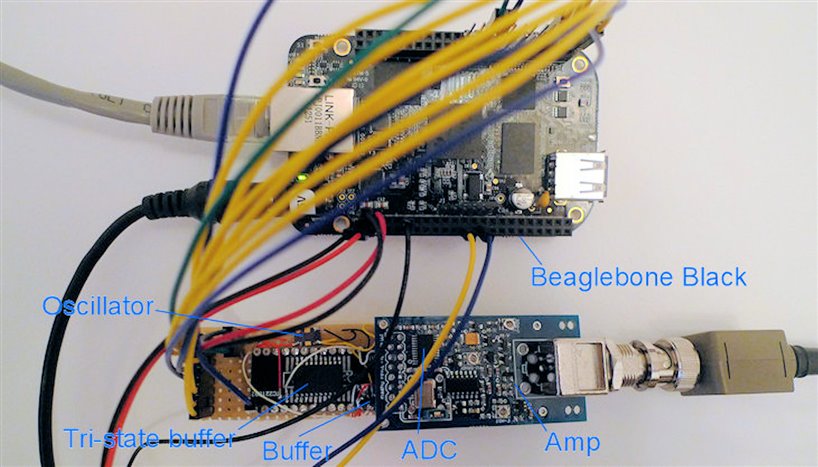
image

A bit more detail:

image

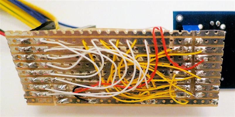
The underside was more untidy!

image


ADC Detail

As mentioned, a ready-built amplifier and ADC board was used. The on-board oscillator was disabled, so that an external one could be fed in. I needed a clock of 20MHz or less, but I only had a 32MHz oscillator at hand and didn't want to wait (and the local Maplin store doesn’t sell any 3.3V-compatible logic to divide by two!) and I’m not entirely sure how long the shared memory write takes, and I did experience lost samples with the 32MHz oscillator. I plan on trying frequencies in the range 14MHz-20MHz to find the upper limit for missing no samples; for further study!

Note that some ADCs will have specific requirements related to the clock and duty cycle.

The ADC on this particular board was ADC08200 but an ADC08100 or ADC08060 could have been used at lower cost).


Buffers

These were extremely important for two reasons. One reason is that the pins to the BBB that I wished to use need to be isolated during power-up, because they are used for selecting the boot method. If there was any unusual level on the pins upon power-up then the BBB will not boot from the eMMC. So, a tri-state buffer is needed.

The other reason is that there is a fair bit of capacitance and it is highly likely that the ADC may not be able to directly drive the pins at high speed. I actually came across this problem while trying to connect a camera to the BBB. I struggled for days without realising that the camera could not support the load. So, the buffers are likely to be essential for most designs using the pins that were selected. I used a 74LVC244A device as a buffer.

Note that the clock also needs a buffer, unless significant jitter is acceptable. No tri-state is required here, so I used a MC74VHC1GT50.


PRU code

The PRU code uses shared memory for communication. I designated a single byte of shared memory to be used for commands. When run, the PRU sits in a loop waiting for the command to instruct it to begin the data capture.  PRU GPI mode is used which allows inputs to be read at the processor speed of 200MHz with no varying latency. Just a few instructions are needed to populate the data into shared memory. No attempt was made to pack the data, and 32-bits are used to store the 8-bit sample. This is not such a bad idea, because in future the ADC could be swapped out to a (say) 10-bit ADC with no code change on the PRU.

There are two PRUs in the AM3359. There are a total of 12 PRU GPI capable pins available that are connected to PRU 1 which are brought out to port 8 on the BBB. So, this means that realistically 10 or 11-bit is about the limit for high-speed parallel ADCs connected in this manner. Still, at (say) 16MHz clock, this would equate to 20Mbytes/sec of data for a 10-bit ADC.

EDIT: See comments section - on PRU0, all 16 pins are in theory available).

The pins used are shared with the HDMI interface; it proved necessary to disable the HDMI interface by recompiling the device tree file in the /boot folder (EDIT: See Brian's comment below for a better method to disable HDMI). Since I wished to display the data using a web browser, I have no issue with losing the HDMI.

Once the data has been captured (2000 samples in this example), the command byte is acknowledged, so that the Linux hosted application can know that the PRU has completed. The PRU now sits and waits for a new instruction from the Linux hosted application.

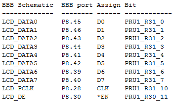
These were the pins used. They were used as D[0..7], CLK and a *EN signal for controlling the octal tri-state buffer.

image


Linux hosted application

The adc_app program is very simple (C code); it downloads the assembled code into PRU1 and executes it. The resultant data in shared memory is dumped to a text file and then the program exits.


Node.js application

The Node.js application creates a HTTP server (no need for apache!) and a Socket.IO connection. This sits and waits for a connection from any web browser. Once it receives a connection, it will send a handshake and then wait for a ‘capture’ command from the web browser. It then calls the adc_app program. Once complete, it opens the file of captured data and transmits it over the Socket.IO connection line-by-line. This is very inefficient, but it is proof-of-concept code that could really be optimised.


Web Page

The web page served up contains some small bits of code to handle the Socket.IO connection and send a ‘capture’ request when a button is clicked and to display the received data with a canvas element and pixel manipulation.


Summary

In conclusion, it is possible to read analog data with low jitter at fairly high speeds without any external FIFO or logic (beyond a simple buffer IC), while continuing to run Linux applications such as a web server. It is also nice that a web-based UI can be rapidly created using Node.js.


Note: It is still for further study how long captures can be sustained and read off by the Linux application without any data loss. If it can be sustained, then it could be useful for SDR applications just about, although a higher speed (and better ADC) would be preferable.


Note2: The waveforms used to test out the system were generated by the same BBB using a low-cost ‘direct digital synthesis’ (DDS) board. That’s a subject for a later date.


Using the code

Disable the HDMI as mentioned in the comments.

You may need to install Socket.IO. Type this to install it:

npm install socket.io


Create a development folder and then the attached code can be unzipped to (say) /home/root/development/adc.


make clean
make
cp BB-BONE-HSADC-00A0.dtbo /lib/firmware/
source install_hsadc_cape.sh
node index.js

Then, navigate to http://xx.xx.xx.xx:8081/index.html


If you want to make subsequent changes, there is a bug in the makefile, and you will need to issue 'make clean' before typing 'make' whenever any change is made in the C code.

If you just want to reassemble the PRU code, type 'make pru' (no need for 'make clean').

Attachments:
adc_v1.zip
  • Sign in to reply

Top Comments

  • Former Member
    Former Member over 12 years ago in reply to bwelsby +2
    Brian Welsby wrote: again are all the pins available? I'm beginning to wonder how long it's going to take for somebody here to decide they want a BBB with a few differences, take the available designs…
  • stanto
    stanto over 11 years ago in reply to morgaine +2
    These values sound very small. Perhaps I have misread but is this relevant ? https://groups.google.com/forum/m/#!topic/beagleboard/Gb6xL7V7Z00
  • morgaine
    morgaine over 12 years ago +1
    After your I2S audio DAC article, I was wondering when the ADC one would appear. In addition to SDR, I'm interested in ADC functionality for the multifunction instrument idea. Since you pointed out that…
Parents
  • morgaine
    morgaine over 12 years ago

    After your I2S audio DAC article, I was wondering when the ADC one would appear. image


    In addition to SDR, I'm interested in ADC functionality for the multifunction instrument idea.


    Since you pointed out that:


    1. the KNJN board is not optimal for several reasons, and
    2. you  also want more ADC width and speed for the future, and
    3. the PRU has plenty of speed in reserve, but
    4. the number of PRU-connected GPIs is limited,


    these four factors seem to combine towards using just 8 GPIs to read in bytes from an external 16:8 selector that samples an ADC of up to 16 bits wide and runs a lot faster.  Because the PRU triggers sampling, only one half of the 16 bits would need to sample and hold while the PRU gets around to reading in the other half, thus saving us an 8-bit register while also allowing the ADC to run faster because its sample acquisition time is overlapped with the PRU read time.


    Or, at the cost of SAH on all 16 bits, the sampler could be fully external and asynchronous w.r.to the PRU's cycle period to give the ADC even more acquisition time, although I'm in two minds about whether this helps since that might require the addition of under-read logic to tell the PRU that a sample was missed..


    Maybe it's too early to be thinking about this without a coffee. image

    • Cancel
    • Vote Up +1 Vote Down
    • Sign in to reply
    • More
    • Cancel
Comment
  • morgaine
    morgaine over 12 years ago

    After your I2S audio DAC article, I was wondering when the ADC one would appear. image


    In addition to SDR, I'm interested in ADC functionality for the multifunction instrument idea.


    Since you pointed out that:


    1. the KNJN board is not optimal for several reasons, and
    2. you  also want more ADC width and speed for the future, and
    3. the PRU has plenty of speed in reserve, but
    4. the number of PRU-connected GPIs is limited,


    these four factors seem to combine towards using just 8 GPIs to read in bytes from an external 16:8 selector that samples an ADC of up to 16 bits wide and runs a lot faster.  Because the PRU triggers sampling, only one half of the 16 bits would need to sample and hold while the PRU gets around to reading in the other half, thus saving us an 8-bit register while also allowing the ADC to run faster because its sample acquisition time is overlapped with the PRU read time.


    Or, at the cost of SAH on all 16 bits, the sampler could be fully external and asynchronous w.r.to the PRU's cycle period to give the ADC even more acquisition time, although I'm in two minds about whether this helps since that might require the addition of under-read logic to tell the PRU that a sample was missed..


    Maybe it's too early to be thinking about this without a coffee. image

    • Cancel
    • Vote Up +1 Vote Down
    • Sign in to reply
    • More
    • Cancel
Children
  • shabaz
    shabaz over 12 years ago in reply to morgaine

    Hi Morgaine,


    You're right, there are 16 available per PRU, but unfortunately on PRU1, 4 of them are being used for the main UART0) and MMC1, which is the eMMC.

    I'm glad you brought up the question, since on PRU0, I just checked, it may be possible to use up all of them! (This would result in MMC0, i.e. the microSD socket) not being usable while the application is running, but this is a small loss. I should have checked in more detail earlier :-)

    I will move my code to PRU0 and confirm 100% if these pins all work ok. Since one pin is needed for receiving the clock, this means 15-bits are usable, which I imagine are quite expensive ADCs at these frequencies :-) I'd be extremely happy with 14 bit or more. This really is awesome if 15-bit is possible.

    • Cancel
    • Vote Up 0 Vote Down
    • Sign in to reply
    • More
    • Cancel
  • Former Member
    Former Member over 11 years ago in reply to shabaz

    A wee while since this discussion took place so I hope I am not annoying people by reviving it.

    Unless I am missing something I can only see 8 PRU0 signals going to the P9 connector and none to P8. The lines going to the MMC0 are not linked to the connectors.

    So far it seems to me that there are 14 signals from PRU1 to P8 (PRU1_30/31_0 to 13) and 8 signals going from PRU0 to P9 (PRU0_30/31_0 to 7).

    The direction of the pins appear to be set by the pin mode selected (mode 5 for output and 6 for input). Am I right in thinking that it means the pin direction cannot be changed on the fly and it is a dts job? That is using PRU instructions to change the pin from an output to an input or vice e versa is not possible. This is a bit of restriction to implementing a bidirectional communication system. I was hoping to use PRU0 one way and PR1 the other but with only 8bits on PRU0 that doesn't leave any room for control signals.

    • Cancel
    • Vote Up +1 Vote Down
    • Sign in to reply
    • More
    • Cancel
  • shabaz
    shabaz over 11 years ago in reply to Former Member

    Hi Sebastian,


    No problem reviving it! You're right, as I understand (I could be wrong), the dts is restrictive if you want bidirectional capability on the fly. You could use the dts to program for one direction, and then change the direction in your code - see here for an example of this (this was in a Linux application, not PRU,  but the registers that need to be programmed are the same).  As you can see from that link, sometimes I've just given up on the dts and directly programmed the pins (It is not always appropriate, but in certain circumstances I think it is ok (e.g. temporary prototyping, or in an environment where you know exactly what is plugged into the BBB).

    • Cancel
    • Vote Up +1 Vote Down
    • Sign in to reply
    • More
    • Cancel
  • Former Member
    Former Member over 11 years ago in reply to shabaz

    Thanks Shabaz.


    Excellent write up by the way.

    I am looking at something robust and relatively simple to implement though as the idea is to interface the BBB with the FPGA board I produce (see: aes220 high speed USB FPGA mini-module if interested). The idea is to have two FIFO in the FPGA to pass data in and out to the BBB as is already implemented in the USB interface. On the BBB side it would be a simple library with functions passing or receiving arrays of bytes to/from the FPGA. I guess I could have two 4 bit buses, that would still give a fast throughput and converting from niblets to bytes is not difficult.

    • Cancel
    • Vote Up +1 Vote Down
    • Sign in to reply
    • More
    • Cancel
  • shabaz
    shabaz over 11 years ago in reply to Former Member

    Hi Sebastien,


    I see, interesting stuff! I think two 4-bit busses would be a good idea, throughput would still be reasonable since the PRU runs at a high speed. Another thing is how long you wish to sustain it for, because the data needs to be read out as well, and the amount of shared mem that is allocated for PRU use that can also be read by applications running on Linux is limited to 12kbyte today. It would be nice to have a higher amount of RAM allocated but that requires some Linux driver expertise.

    • Cancel
    • Vote Up +1 Vote Down
    • Sign in to reply
    • More
    • Cancel
element14 Community

element14 is the first online community specifically for engineers. Connect with your peers and get expert answers to your questions.

  • Members
  • Learn
  • Technologies
  • Challenges & Projects
  • Products
  • Store
  • About Us
  • Feedback & Support
  • FAQs
  • Terms of Use
  • Privacy Policy
  • Legal and Copyright Notices
  • Sitemap
  • Cookies

An Avnet Company © 2025 Premier Farnell Limited. All Rights Reserved.

Premier Farnell Ltd, registered in England and Wales (no 00876412), registered office: Farnell House, Forge Lane, Leeds LS12 2NE.

ICP 备案号 10220084.

Follow element14

  • X
  • Facebook
  • linkedin
  • YouTube