

 |  |  |
| BUY NOWBUY NOW |
| Kit Overview | Development Tools | Technical Documents | Video | Features | Kit Contents |
Overview
The Altera DK-DEV-4SGX230N DK-DEV-4SGX230N Stratix IV GX FPGA Development Kits deliver a complete system-level design environment that includes both the hardware and software needed to immediately begin developing Stratix IV GX FPGA designs. The PCI-SIG-compliant board and the one-year license for the Quartus II software provide everything you need to begin developing custom Stratix IV GX FPGA designs.
The following list describes what you can accomplish with the kit:
- Develop and test PCI Express 2.0 (up to x8 lane) endpoint and root port designs
- Develop and test memory subsystems consisting of DDR3 and QDR II+ memory
- Build designs capable of migrating to Altera's low-cost HardCopy IV ASICs
- Add other Stratix IV GX FPGA-supported protocol interfaces such as 10-Gbps Ethernet, CPRI, OBSAI, SAS/SATA, Serial RapidIO.
- Take advantage of the modular and scalable design by using the high-speed mezzanine card (HSMC) connectors to interface to over 20 different HSMCs provided by Altera partners, supporting protocols such as Serial RapidIO, 10 Gigabit Ethernet, SONET, Common Public Radio Interface (CPRI), Open Base Station Architecture Initiative (OBSAI) and others
- Develop FPGA designs for cost-sensitive applications
- Measure the FPGA's power consumption
Key Applications: Wireless market, Wireline market, Military market, Broadcast market, DSP, Embedded processing, Memory interfaces and ASIC prototyping.
Development Tools
Software Development Tools:
| Tool Type | Supplier | Supported Family | MPN | Description |
|---|---|---|---|---|
| IDE | Altera | ALL Altera Devices | Altera Quartus II | It's the industry's number one software in performance and productivity for CPLD, FPGA, and HardCopy ASIC designs. The Altera Quartus II software, the industry's number one software in performance and productivity for CPLD, FPGA, and HardCopy ASIC designs. Learn More |
Hardware Development Tools:
| Tool Type | Supplier | Support?ed Family | MPN | Description |
|---|---|---|---|---|
| Download Cable | Altera | ALL Altera Devices | PL-BYTEBLASTER2NPL-BYTEBLASTER2N | The ByteBlaster II enables a PC to configure or program Altera devices. The download cable drives configuration or programming data using a standard parallel printer port from the PC. |
| Download Cable | Altera | ALL Altera Devices | PL-USB-BLASTER-RCNPL-USB-BLASTER-RCN | The USB-Blaster drives configuration or programming data from the PC to configure or program Altera devices. The download cable interfaces to a standard USB PC port. |
| Download Cable | Altera | ALL Altera Devices | PL-ETH2-BLASTERPL-ETH2-BLASTER | The EthernetBlaster can receive configuration or programming data from the Ethernet network to remotely configure or program Altera devices. The communications cable connects to a standard Ethernet network port with an RJ-45 connector. |
Technical Documents
Learning Center
| Type | Description |
|---|---|
| User Guide | Altera: Quick Start Guide for Stratix IV GX Development Kit |
| User Guide | Altera: User Guide for Stratix IV GX FPGA Development Kit |
| Reference Manual | Altera: Reference Manual for Stratix IV GX FPGA Development Board |
| Reference Manual | Altera: Reference Manual for Stratix IV Device Handbook |
| Product Brief | Altera: Product Brief for Stratix IV GX FPGA Development Kit |
| Datasheet | Altera: Datasheet for Stratix IV Device Handbook |
| Revision Note |
Design Elements
| Type | Description |
|---|---|
| Schematics | Altera: Schematics File for DK-DEV-4SGX230N Dev Kit |
| Layout | Altera: Layout File for DK-DEV-4SGX230N Dev Kit |
| BOM | Altera: BOM File for DK-DEV-4SGX230N Dev Kit |
| Application Library | Altera: Software Code for DK-DEV-4SGX230N Dev Kit |
Video
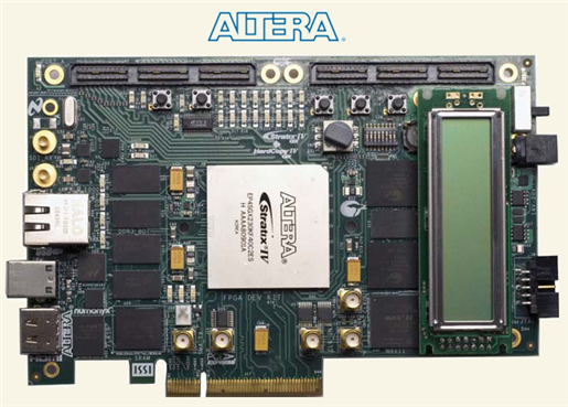
Kit Features
The board features the following major component blocks:
- EP4SGX230KF40 FPGA in the 1517-pin FineLine BGA Package
- 228,000 LEs
- 91,200 adaptive logic modules (ALMs)
- 17,133 Kbit on-die memory
- 126.5 Gbps transceivers (PMA only)
- 2 PCI Express hard IP blocks
- 8 phase locked loops (PLLs)
- 1288 18x18 multipliers
- 0.9-V core power
- MAX II CPLD EPM2210EPM2210 System Controller in the 256-pin FineLine BGA Package
- 1.8-V core power
- FPGA Configuration Circuitry
- MAX II CPLD EPM2210 System Controller and Flash Fast Passive Parallel (FPP) configuration
- On-Board USB-BlasterTM for use with the Quartus II Programmer
- MAX
- On-Board Clocking Circuitry
- 50-MHz/100-MHz/125-MHz/148.5-MHz/155.52-MHz/156.25-MHz oscillator
- SMA connectors for external clock input
- SMA connectors for clock output
- Memory devices
- 512-Mbyte DDR3 SDRAM with a 64-bit data bus (bottom port)
- 128-Mbyte DDR3 SDRAM with a 16-bit data bus (top port)
- Two 4-Mbyte QDRII+ SRAMs with 18-bit data buses
- 2-Mbyte SSRAM with 36-bit data buses
- 64-Mbyte synchronous flash
- General User I/O
- 16 user LEDs
- Two-line character LCD display
- One configuration done LED
- One transmit/receive LED (TX/RX) per HSMC interface
- Four PCI Express LEDs
- Four Ethernet LEDs
- Push-Button Switches
- One user reset (CPU Reset)
- One configuration reset
- Three general user push-button switches
- DIP Switches
- Eight user DIP switches
- Eight MAX II control DIP switches
- Power
- 16-V – 20-V DC input
- PCI Express edge connector power
- On-Board power measurement circuitry
- Mechanical
- PCI Express half-length full-height (6.6” x 4.376”)
- PCI Express chassis or bench-top operation
Kit Contents
The Altera DK-DEV-4SGX230NDK-DEV-4SGX230N Development kit supplied with below contents:
Hardware:
- Stratix IV GX FPGA development board - A development platform that allows you to develop and prototype hardware designs running on the Stratix IV GX EP4SGX230 FPGA.
- HSMC loopback board - A daughtercard that allows for loopback testing all signals on the HSMC interface using the Board Test System
- HSMC debug breakout board - A daughtercard that routes 40 CMOS signals to a 0.1" header and adds 20 LEDs to the remaining 40 CMOS signals.
- Power supply and cables - The kit includes the following items:
- Power supply and AC adapters for North America/Japan, Europe, and the United Kingdom USB cable
- Ethernet cable
- 75 Ω SMB video cable
Software:
- Quartus II Subscription Edition Software
- Stratix IV GX FPGA Development Kit Installer
 |  |  |