


1. Introduction
I've recently started testing out the latest version (v8.3.1) of EAGLE Premium, and one of the features I was really interested to try out since I first saw v8 earlier in the year was the BGA Router. Breaking out BGA's is time consuming so if that effort can be reduced then that's a big bonus. On the other hand, I don't like autorouters and the results are never anything close to the standards I set for myself when routing by hand, in fact many of the boards I do would be impossible to autoroute satisfactorily, so any automatic BGA breakout is going to have to do a better job than your typical autorouter does. So lets see what happened when I devised some tests and took the BGA Router for a spin!
Spoiler Alert: You will have to put some effort into setting things up and do some manual clean up in order to get a satisfactory result in the end.
2. The Test Schematic
I decided that to keep things simple I would create a very specific test schematic which would allow me to focus just on the BGA breakout without any other distractions going on around the board. I created a simple schematic which has an FPGA in a 256-ball package, with all the I/O pins connected to surface mount test points and all the power pins connected up to appropriate power rails. The idea being it would allow me to determine how nicely it routes out and how well it deals with the very important task of connecting power to the device, without any other distractions with unrelated components and routing. In this example I have ignored decoupling capacitors but these would be placed on the bottom side of the board anyway and likely wouldn't have too much effect on the placement of any vias if placed correctly.
3. Setting Up the Board
For this test I have chosen to have a 6 layer board. I'll use the inner two layers for GND and +3V3 and then have an area fill on the bottom layer for +1V0. I could likely do a split power plane on layer 4 for +3V3 and +1V0 but to keep it simple I will just put it on the bottom layer. I want to have microvias available for layers 1-2, 2-3, 14-15, and 15-16 as well as buried vias. In order to set this up I need to go into the DRC and configure the layer setup as follows:
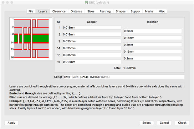
Note: Ignore the Copper and Isolation thickness settings as I haven't set these up as they not going to affect our example.
I also set the clearances to be 4mil, minimum track setting to 4mil, microvia drill to 4mil, regular via drill to 10 mil etc to enable sensible via geometries. I won't include details here as they are just part of normal routing setup and not specific to using the BGA router. However, you must make sure you have these set up properly so that you can route our from the BGA without incurring DRC errors otherwise it will not route.
4. Manually Breaking Out the BGA as a Point for Comparison
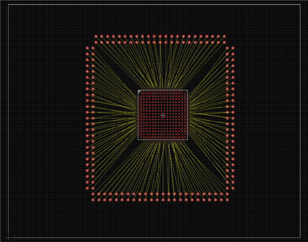
After setting up the board I decided that the first thing I should do would be to manually route out the BGA so that I can give a baseline for comparing the results from the BGA Router. As this is a relatively small BGA at just 256 balls with a very generous 1mm pitch this didn't take too long to achieve. Setting the grid to 0.5mm I started by breaking out the outer row of balls all the way round on the top layer, then continued round and did the second row. There were still available routing channels so I went ahead and routed as many from the next row around as I could through the remaining routing channels. After routing out the top layer we have the following:
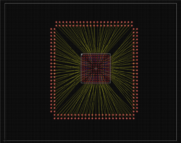
Now it was time for the layers which require vias. The test board is set up for microvias and we shall use via-in-pad as this is quite a common technique when routing out BGA's. Setting the via drill to 4mil we proceed as before working around the device and adding in the routes into all the available routing channels on layer 2. The only caveat here is that if there is a BGA pad on the top layer relating to one of the power or ground pins then we shall not route underneath that and will leave the routing channel free. I could have put the power breakout in first but I decided to leave that until last to keep the pictures clearer for illustrating the breakout of the main I/O signals. The result of routing out on layer 2 is as follows:
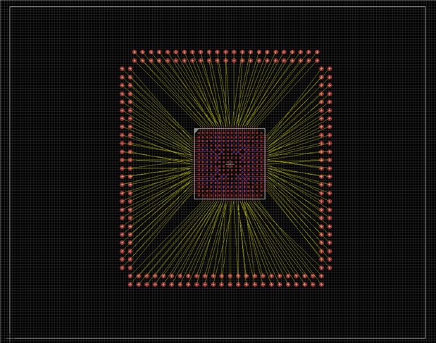
We still have some unrouted I/O pins. There aren't many (a handful for each side) and they could be routed out on layer 3 using stacked microvias underneath the BGA pads, but I want to keep layer 3 clear and unbroken for the GND signals (slots in the GND plane where other traces go has negative impacts on signal integrity as signal return currents have to find a less direct path). What I chose to do instead was to have staggered vias, a microvia in the BGA pad to layer 2 and then a 2-15 via offset from the microvia and route the signals out on layer 15. I approached this in exactly the same way as routing out the other I/O signals and worked my way around the device until they were all routed in. The result of these final I/O signals being routed out is as follows:
Next it's the turn of the power and ground signals. Connecting up the GND net is easy, I simply put stacked microvias 1-2 and 2-3 to connect the GND pads up to the GND polygon on layer 3. For +3V3 and +1V0 I used a combination of microvias and staggered 2-15 vias to get these signals to the polygons on their respective layers. The finished result of manually breaking out the BGA is as follows:
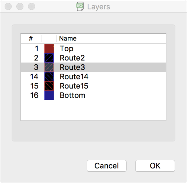
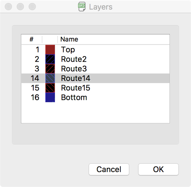
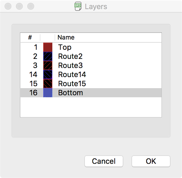
5. Configuring the BGA Router Settings
The first time I tried the BGA Router, I set up the board and ran the BGA Router and just set it off running without any additional configuration. It took almost 4 hours and the results were less than stellar. This was however to be expected as the router didn't have enough information by default to be able to do a good job. First things first, set the various nets to only route on their appropriate layers. Open up the BGA Router and the BGA Settings window will be displayed as follows:
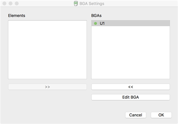
Press the Edit BGA button and the following window will be displayed:
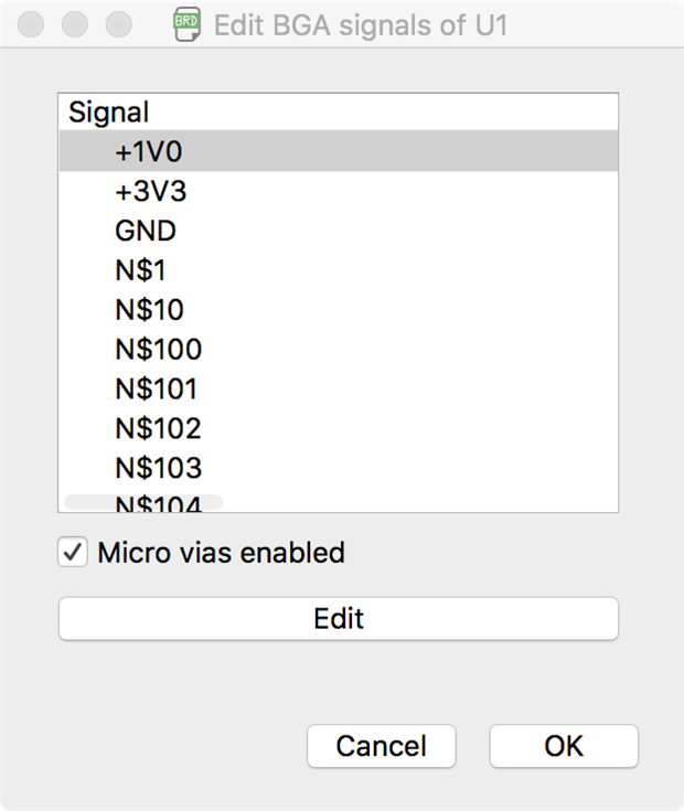
The I/O's will be allowed to route on layers 1, 2 and 15 so we will group select the I/O pins and press edit to alter the setup. We then select the layers as required and press OK. The layer setup window is as follows:
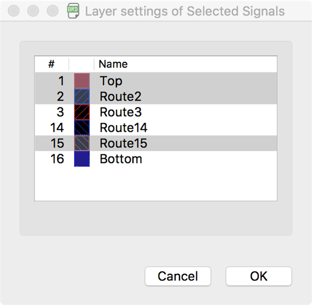
We repeat the same for GND, +3v3, and +1V0 with the windows as follows:
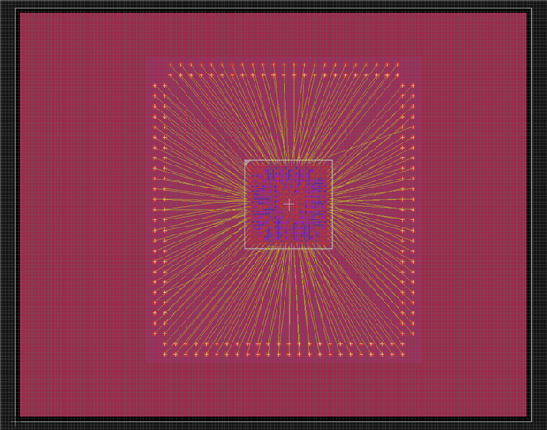
6. The finished Result
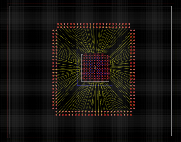
After letting the BGA Router finish its routing run which took around 10 minutes (I didn't time it unfortunately) the result was as shown below:
7. Comparison with Hand Routed BGA Breakout
On first glance the BGA Router seems to have done ok. It's used the correct layers for the IO, the same as I had used in my manual breakout, and although they are a little less tidy than my hand crafted version they are all in and going in the right direction which is nice.
On closer inspection of the power net routing though we soon uncover something a little wrong....
Whilst I have told it to only route the GND, +3V3, and +1V0 on layers 3, 14 and 16 respectively, it has decided to route between BGA pads on layer 1 to connect some of these together and then only going down to the plane with vias in a limited number of places. This is a little disappointing and limits the usefulness of the BGA Router as it stands but this is something that I am sure Autodesk will be able to fix quite easily in a future update.
It is also not possible to control the via type and breakout type to give me the same control as if I am manually routing out the BGA. For example, I might want to use microvias but not have via in pad. Currently with the BGA Router, if I select microvia it will use via in pad, unless standard vias will fit in the space between pads and then it will use those instead in a staggered breakout arrangement. It's not possible to have a staggered breakout with micrivias. This isn't the end of the world, but again is a limiting factor if you are trying to keep the board technology as manufacturer friendly as possible.
8. Summary and Conclusions
The BGA Router is an interesting addition to EAGLE. It is better than I had initially anticipated based on my lack of fondness for autorouters in general, and whilst it doesn't do a perfect job, as good as I can do manually, it is certainly usable and I think with some more development could become a very powerful tool to speed up the layout process. Currently, it's good for breaking out I/O nets, although it doesn't do as neat of a job as I can do by hand if you compare my original hand routed breakout against the result from the BGA Router.
Where it currently falls apart is routing out power nets. Connecting power pads together with traces on the top layer rather than taking each one down to their respective plane with vias is not acceptable, especially when routing for those nets have been turned off for the top layer. So for now, I will be either sticking to routing the power nets by hand or going in and doing lots of manual fix ups afterwards.
In general though, on a large BGA, if you don't have the time to spend manually to make it look pretty, breaking out just I/O connections with the BGA Router in EAGLE v8 could be a significant time saver. I think there are definitely things they can do to improve things, more info about why things didn't route out correctly for example and more guidance on getting the setup right in the first place, but I think as it is it is still a valuable tool to have to hand.
One other word of warning. If you try to use this tool and you already have some routing on your BGA, you will very likely end up with EAGLE crashing and closing. This is a known issue with the current version (v8.3.1) which I am sure will be corrected in a subsequent release.
This concludes the my overview of getting the BGA Router of EAGLE v8 to behave. Let me know what you think in the comments below and if you have any questions please feel free to ask!
Top Comments