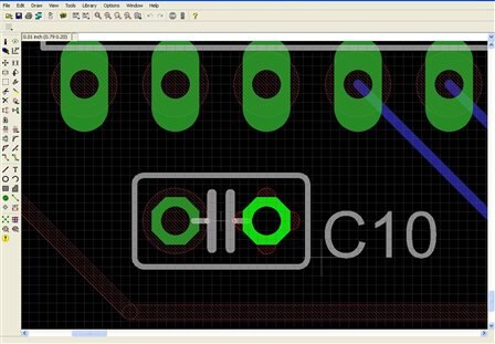
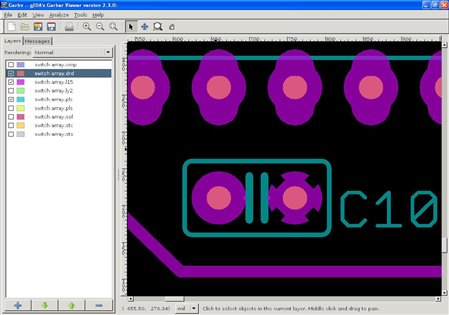
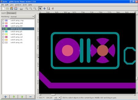
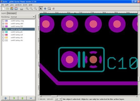
I am making my first board with inner supply layers, and when I make the cam
files, the component pads are showin up in the inner layers. Since the
supply layers are inverted, this makes an area around the thru-holes with no
copper, and none of my power or ground connections are being made. How do I
keep the pads from showing up in my supply layers?