


Hi,
Hoping some Eagle experts can help me understand either what I am doing wrong or what I need to do to get this completed. I am creating a PCB antenna using a coplanar waveguide in eagle and I cannot work out if I am doing it properly as I cannot get the isolation level correct around the transmission line. In order to create the correct 50 Ohm impedance.
- I know I need a 0.74mm transmission line from the chip through my Pi network to the antenna
- I know I need an isolation of 0.11mm to the GND
- I will be using 1.6mm PCB with a dielectric constant of 4.6.
Please see the AppCad calculations below.

To build this layout in eagle I have researched online to understand I can try it several ways. But I am being checkmated each time I try.
First way: Use a Wire
If I use a wire to connect the airwire, I can define the width to be 0.74mm quite easily. However, if I do this it uses the DRC clearance level of 0.15mm. This 0.15 level will change my impedance. I can see the settings at 0.15mm under Edit -> Design Rules -> Clearance Tab is set at 0.15mm. If I change the grid to 0.11mm I can see that the distance to ground is 0.15mm using this method. Then I looked at setting this transmission line as a different Net Class under Edit -> Net Classes. But one cannot set the isolation around the wire. One can set the width of the wire in the net class but not the isolation.
Second Way:
So then I tried to create a polygon. I made the width 0.37 and worked my way between the antenna point below and the left hand edge of my Pi network (C15).I then continued between inductor L4 and C16. By setting the grid to 0.01 and being careful I can see that I can make a polygon exactly 0.74mm wide and give it a 0.11mm isolation in the settings.

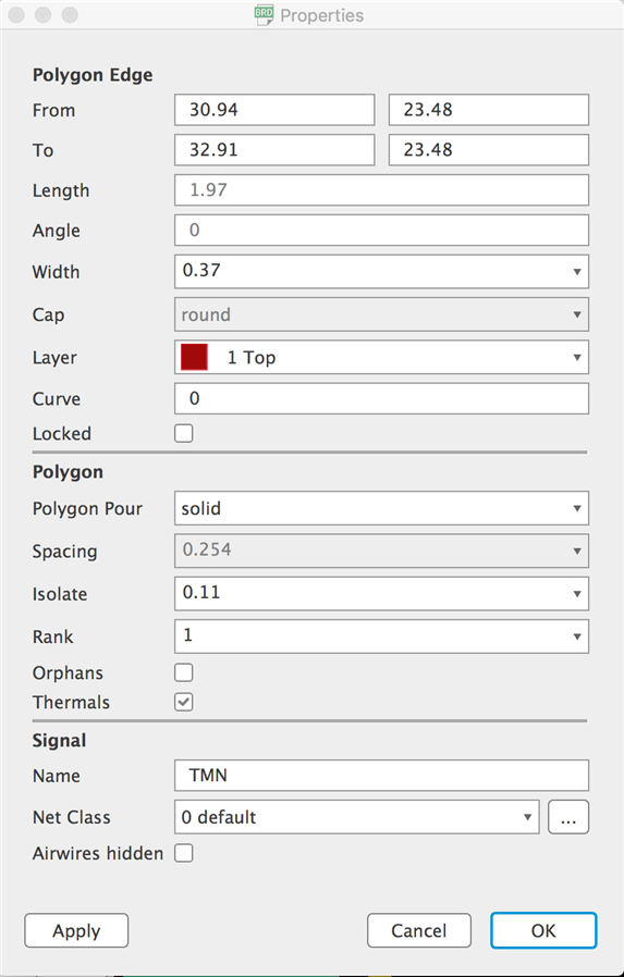
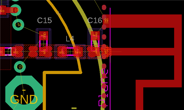
however when I ratsnest it ignores the polygons and the isolation and fills it all in...

If I use Properties -> Convert To Wires, it once again uses the DRC at 0.15mm, which is checkmate, so I can't use that route.
Question One: How do I get the ratsnest to respect the polygons that I have built to be the transmission line to the antenna?
Question Two: The autoroute command will not complete unless I connect the air wires along the transmission line. Do I do this underneath the polygon?
Apologies if I am missing something simple and this is a silly question, however I am quite stumped by it and I've tried most every method I can think of.
Best,
SteadyD
