element14 Community
element14 Community
    Register Log In
  • Site
  • Search
  • Log In Register
  • Community Hub
    Community Hub
    • What's New on element14
    • Feedback and Support
    • Benefits of Membership
    • Personal Blogs
    • Members Area
    • Achievement Levels
  • Learn
    Learn
    • Ask an Expert
    • eBooks
    • element14 presents
    • Learning Center
    • Tech Spotlight
    • STEM Academy
    • Webinars, Training and Events
    • Learning Groups
  • Technologies
    Technologies
    • 3D Printing
    • FPGA
    • Industrial Automation
    • Internet of Things
    • Power & Energy
    • Sensors
    • Technology Groups
  • Challenges & Projects
    Challenges & Projects
    • Design Challenges
    • element14 presents Projects
    • Project14
    • Arduino Projects
    • Raspberry Pi Projects
    • Project Groups
  • Products
    Products
    • Arduino
    • Avnet & Tria Boards Community
    • Dev Tools
    • Manufacturers
    • Multicomp Pro
    • Product Groups
    • Raspberry Pi
    • RoadTests & Reviews
  • About Us
    About the element14 Community
  • Store
    Store
    • Visit Your Store
    • Choose another store...
      • Europe
      •  Austria (German)
      •  Belgium (Dutch, French)
      •  Bulgaria (Bulgarian)
      •  Czech Republic (Czech)
      •  Denmark (Danish)
      •  Estonia (Estonian)
      •  Finland (Finnish)
      •  France (French)
      •  Germany (German)
      •  Hungary (Hungarian)
      •  Ireland
      •  Israel
      •  Italy (Italian)
      •  Latvia (Latvian)
      •  
      •  Lithuania (Lithuanian)
      •  Netherlands (Dutch)
      •  Norway (Norwegian)
      •  Poland (Polish)
      •  Portugal (Portuguese)
      •  Romania (Romanian)
      •  Russia (Russian)
      •  Slovakia (Slovak)
      •  Slovenia (Slovenian)
      •  Spain (Spanish)
      •  Sweden (Swedish)
      •  Switzerland(German, French)
      •  Turkey (Turkish)
      •  United Kingdom
      • Asia Pacific
      •  Australia
      •  China
      •  Hong Kong
      •  India
      •  Japan
      •  Korea (Korean)
      •  Malaysia
      •  New Zealand
      •  Philippines
      •  Singapore
      •  Taiwan
      •  Thailand (Thai)
      •  Vietnam
      • Americas
      •  Brazil (Portuguese)
      •  Canada
      •  Mexico (Spanish)
      •  United States
      Can't find the country/region you're looking for? Visit our export site or find a local distributor.
  • Translate
  • Profile
  • Settings
Autodesk EAGLE
  • Products
  • More
Autodesk EAGLE
EAGLE User Support (English) Design a new part with Twin pads for multiple package
  • Blog
  • Forum
  • Documents
  • Events
  • Polls
  • Files
  • Members
  • Mentions
  • Sub-Groups
  • Tags
  • More
  • Cancel
  • New
Join Autodesk EAGLE to participate - click to join for free!
Actions
  • Share
  • More
  • Cancel
Forum Thread Details
  • Replies 9 replies
  • Subscribers 189 subscribers
  • Views 792 views
  • Users 0 members are here
  • packs
  • frontpage
Related

Design a new part with Twin pads for multiple package

e14 Contributor
e14 Contributor over 10 years ago

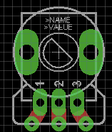
Hi, i'm trying to make a new package for a 3pin potentiometer that come in two different version.

As now i've douplicated the pins, 1 1* 2 2* 3 3* and connected them in the schematic, two by two.

In the package i've connected the pins with top and bottom traces, but i would like to know if there is a better solution, maybe with a custom pad with milling, tcream e tstop.

Here is an example:
image

  • Sign in to reply
  • Cancel
  • e14 Contributor
    e14 Contributor over 10 years ago in reply to rachaelp

    You are assuming correctly, the wires between pads still shown after ratsnest, so i am going with pcb traces as you suggest, it works without pain. I had that width problem when i've used custom pads too, i've retraced the shape of the two pads and the connection with polygons on pad's layer and DRC had allert me with that width problem on that side and the same opposite side in the very right pad.

    • Cancel
    • Vote Up 0 Vote Down
    • Sign in to reply
    • Cancel
  • rachaelp
    rachaelp over 10 years ago in reply to e14 Contributor

    I'm not sure why you are getting just that one width violation with the polygons, I've seen that occasionally before and it seemed random to me when it would occur and I never resolved why. The thing that stands out though is in your pictures the air wires between the pairs of pads are still showing. I assume these are still showing after pressing Ratsnest? It might be quicker to just go with wiring them up in the layout if this solution is proving problematic.

    • Cancel
    • Vote Up 0 Vote Down
    • Sign in to reply
    • Cancel
  • e14 Contributor
    e14 Contributor over 10 years ago in reply to e14 Contributor

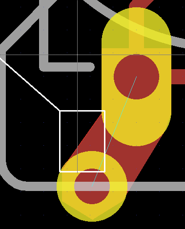
    With polygon instead i have a "width" problem, just in this side.

    image

    • Cancel
    • Vote Up 0 Vote Down
    • Sign in to reply
    • Cancel
  • e14 Contributor
    e14 Contributor over 10 years ago in reply to rachaelp

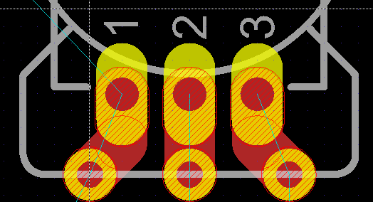
    I've tryed with traces on package first but i have an overlap error on pads running DRC and the pads are not connected, they result as unrouted, i'll try with polygos thank you.

    image

    • Cancel
    • Vote Up 0 Vote Down
    • Sign in to reply
    • Cancel
  • rachaelp
    rachaelp over 10 years ago in reply to e14 Contributor

    I'd probably look to do it with drawing polygons I think, making sure the centres of the real pads fall within the drawn polygons.


    Best Regards,


    Rachael

    • Cancel
    • Vote Up 0 Vote Down
    • Sign in to reply
    • Cancel
  • e14 Contributor
    e14 Contributor over 10 years ago in reply to rachaelp

    The board as now is tiny, but i am curious how to connect two pads in the package, in the board the center of the pad hook the trace but this do not happen in the package editor, do you have any suggestion?


    Regards.

    • Cancel
    • Vote Up 0 Vote Down
    • Sign in to reply
    • Cancel
  • rachaelp
    rachaelp over 10 years ago in reply to e14 Contributor

    You're welcome, glad to be able to help :-)


    With regards to where you should connect the sets of pads, to be honest it probably doesn't really matter that much especially if this is a one-off for a specific project. Doing it in the package will mean they are always connected up automatically every time you put the part on a board and you can move them around as one in the layout which makes things a little easier especially if you have a lot of them on the board but you need to make sure that it actually recognizes your connections in the board and doesn't still leave you with air wires. If it's just one or two on a one-off board I would be tempted to just wire them up in the layout.


    Best Regards,


    Rachael

    • Cancel
    • Vote Up 0 Vote Down
    • Sign in to reply
    • Cancel
  • e14 Contributor
    e14 Contributor over 10 years ago in reply to rachaelp

    This is exactly what i was searching for.

    Thankyou very much, you saved me a lot of stress, i really didn't find a reference about multiple selection.

    So do you suggest to wire up the pins on the board or in the package?


    Best Regards.

    • Cancel
    • Vote Up 0 Vote Down
    • Sign in to reply
    • Cancel
  • rachaelp
    rachaelp over 10 years ago

    Hello,


    I think I have understood what you are trying to achieve, i.e you want to put a single part down on the board which has dual footprints so you can use two variants of the part on the same board layout?


    If this is the case I don't think you're too far off on this although you don't need to have duplicated pins on the schematic, just put pins 1, 2 and 3 on there. In the package put all your pads down and wire them up as you have at the moment. Then when you assign symbol pins to package pads, you assign each symbol pin to BOTH package pads. I.e. select symbol pin 1 in the left pane and multi-select pads 1 and 1* in the middle pane and the click connect. Repeat for pins 2 and 3.


    Using wires rather than creating custom pads to connect the pairs within the symbol I think is fine. You don't need to do anything else with tcream, tstop etc as it wont need anything different to what is provided by the 6 pads you initially placed. The traces between them need to have solder mask and there would be no paste there.


    Best Regards,


    Rachael

    • Cancel
    • Vote Up 0 Vote Down
    • Sign in to reply
    • Cancel
element14 Community

element14 is the first online community specifically for engineers. Connect with your peers and get expert answers to your questions.

  • Members
  • Learn
  • Technologies
  • Challenges & Projects
  • Products
  • Store
  • About Us
  • Feedback & Support
  • FAQs
  • Terms of Use
  • Privacy Policy
  • Legal and Copyright Notices
  • Sitemap
  • Cookies

An Avnet Company © 2026 Premier Farnell Limited. All Rights Reserved.

Premier Farnell Ltd, registered in England and Wales (no 00876412), registered office: Farnell House, Forge Lane, Leeds LS12 2NE.

Follow element14

  • X
  • Facebook
  • linkedin
  • YouTube