


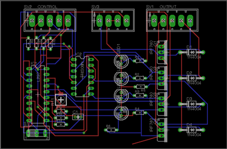
Hello All. This is my first attempt at using Eagle software to develop a printed circuit board. This project is for the purpose of jumping into the program to gain a foothold on learning it's ways. I've come accross something that I don't understand so I've come asking for some help. As seen in the board image, IC1 (L297) is a DIP. It looks to me that pins on both sides of the chip are shorted to adjacent pins. Anyone have an idea of what's going on? Thanks. - Scotty

Message was edited. Inserted new images in hopes of better resolution.

