Hi
I have routed my pcb with Router and everything looks fine.
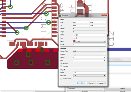
I want to add a heatsinker to some of the pins of a IC by creating a polygon of copper on each side of the PCB close to the IC pin.
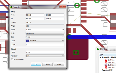
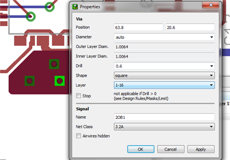
I connect these polygons with a number of vias and attach the vias to the IC pin by givign the the vias and copper polygon the
same net name as the IC pin
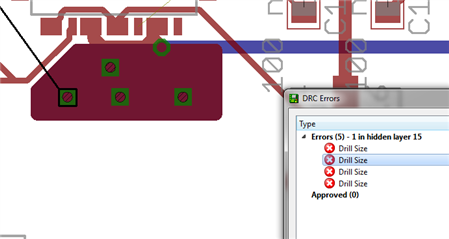
However the Drc command generate a "drill error" for each of the via's.
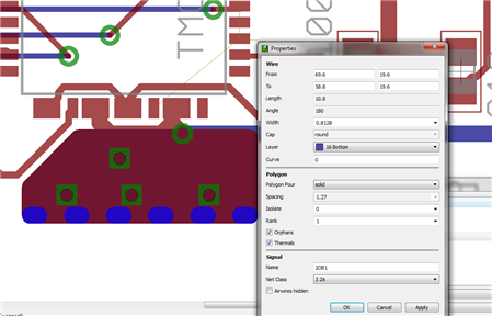
1) Create a polygon in copper on both side of the PCB
2) Place a number of vias inside this polygon of copper
3) Set the Net class name of the vias and copper polygon to the same net class name as the pin
4) Run "Drc"
It seems that the copper polygon's have painted copper over the whole of the vias and therefore the error is reported.
How do I avoid this error message ?
Why do the copper polygon paint over the vias ?
Should I instead set the via's at the edge of the copper polygon or is there other ways of doing it ?
Regards