

Hi
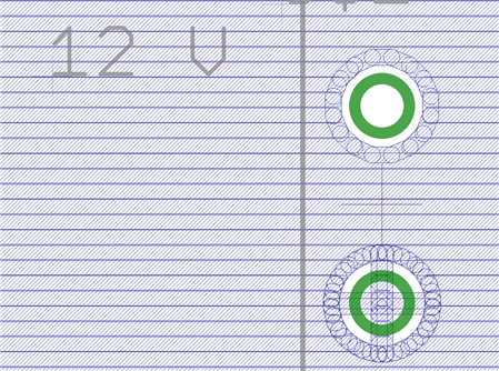
If I have a 4 layer pcb with one layer for GND and connect vias to the GND plane it all looks fine, like this

The GND plane "connect to the via all the way around
however, when I connect the GND pin of the power supply connector to the GND plane the connections is not done "all the way around" but with 4 smaller stripes of copper, like this (lower green circle)
Why do it does that ?
Will it be connected all the way around in the production ?
The reason I am asking is that this will be the weak chain in how much current can be passed via the GND plane,
It is not the width of the wires between components in Top/Bottom layer but it is these 4 small wires and their thickness that decide it.
Even if I choose 140 um copper in all layers, calculate the maximum current along the normal Via's circumference and the width of the wires in top/bottom layers it is still these 4 wires that limit the current.
Regards
