element14 Community
element14 Community
    Register Log In
  • Site
  • Search
  • Log In Register
  • Community Hub
    Community Hub
    • What's New on element14
    • Feedback and Support
    • Benefits of Membership
    • Personal Blogs
    • Members Area
    • Achievement Levels
  • Learn
    Learn
    • Ask an Expert
    • eBooks
    • element14 presents
    • Learning Center
    • Tech Spotlight
    • STEM Academy
    • Webinars, Training and Events
    • Learning Groups
  • Technologies
    Technologies
    • 3D Printing
    • FPGA
    • Industrial Automation
    • Internet of Things
    • Power & Energy
    • Sensors
    • Technology Groups
  • Challenges & Projects
    Challenges & Projects
    • Design Challenges
    • element14 presents Projects
    • Project14
    • Arduino Projects
    • Raspberry Pi Projects
    • Project Groups
  • Products
    Products
    • Arduino
    • Avnet & Tria Boards Community
    • Dev Tools
    • Manufacturers
    • Multicomp Pro
    • Product Groups
    • Raspberry Pi
    • RoadTests & Reviews
  • About Us
    About the element14 Community
  • Store
    Store
    • Visit Your Store
    • Choose another store...
      • Europe
      •  Austria (German)
      •  Belgium (Dutch, French)
      •  Bulgaria (Bulgarian)
      •  Czech Republic (Czech)
      •  Denmark (Danish)
      •  Estonia (Estonian)
      •  Finland (Finnish)
      •  France (French)
      •  Germany (German)
      •  Hungary (Hungarian)
      •  Ireland
      •  Israel
      •  Italy (Italian)
      •  Latvia (Latvian)
      •  
      •  Lithuania (Lithuanian)
      •  Netherlands (Dutch)
      •  Norway (Norwegian)
      •  Poland (Polish)
      •  Portugal (Portuguese)
      •  Romania (Romanian)
      •  Russia (Russian)
      •  Slovakia (Slovak)
      •  Slovenia (Slovenian)
      •  Spain (Spanish)
      •  Sweden (Swedish)
      •  Switzerland(German, French)
      •  Turkey (Turkish)
      •  United Kingdom
      • Asia Pacific
      •  Australia
      •  China
      •  Hong Kong
      •  India
      •  Japan
      •  Korea (Korean)
      •  Malaysia
      •  New Zealand
      •  Philippines
      •  Singapore
      •  Taiwan
      •  Thailand (Thai)
      •  Vietnam
      • Americas
      •  Brazil (Portuguese)
      •  Canada
      •  Mexico (Spanish)
      •  United States
      Can't find the country/region you're looking for? Visit our export site or find a local distributor.
  • Translate
  • Profile
  • Settings
Autodesk EAGLE
  • Products
  • More
Autodesk EAGLE
EAGLE User Support (English) Have a question about CadSoft EAGLE?  Ask our Expert, Jorge!
  • Blog
  • Forum
  • Documents
  • Events
  • Polls
  • Files
  • Members
  • Mentions
  • Sub-Groups
  • Tags
  • More
  • Cancel
  • New
Join Autodesk EAGLE to participate - click to join for free!
Actions
  • Share
  • More
  • Cancel
Forum Thread Details
  • Replies 126 replies
  • Subscribers 200 subscribers
  • Views 10898 views
  • Users 0 members are here
  • our
  • have
  • expert
  • eagle?
  • jorge!
  • ask
  • a
  • cadsoft
  • about
  • question
Related

Have a question about CadSoft EAGLE?  Ask our Expert, Jorge!

Jorge_Garcia
Jorge_Garcia over 13 years ago

If you have questions about CadSoft EAGLE, please click here to post your question!


If you'd rather browse other member's questions you can read the CadSoft EAGLE Forums for past questions and answers. Enjoy!


richardhammerl.png


Jorge Garcia

I'm a young engineer with extensive experience working on EAGLE. My interests include Power Supply design and LED solid state lighting, and I'm always impressed by a well designed PCB.


If not already, you'll need to

image or image


to ask your question.

Otherwise, click reply below.

  • Sign in to reply
  • Cancel
Parents
  • e14 Contributor
    e14 Contributor over 12 years ago

    Hi Jorge,


    I am a new user to Eagle and I am having a hard time with a schematic. I had created some components which I recreated after I learned the hard lesson of schematic view's limitation to 0.1" grid snapping :-(

    After implementing the new components and running ERC, all nets on one IC still show "net N$ overlaps pin". What can I do to fix this?

    Thanks in advance!

    • Cancel
    • Vote Up 0 Vote Down
    • Sign in to reply
    • Cancel
  • e14 Contributor
    e14 Contributor over 12 years ago in reply to e14 Contributor

    Am 22.05.2014 06:11, schrieb J Chop:

    Hi Jorge,


    I am a new user to Eagle and I am having a hard time with a schematic. I

    had created some components which I recreated after I learned the hard

    lesson of schematic view's limitation to 0.1" grid snapping image

    After implementing the new components and running ERC, all nets on one

    IC still show "net N$ overlaps pin". What can I do to fix this?

    Thanks in advance!


    --

    To view any images and attachments in this post, visit:

    http://www.element14.com/community/message/113585


    You can use in symbol-editor :


    RUN snap-pin-in-symbol.ulp


    in schematic-editor:


    RUN snap-on-grid-sch.ulp


    ***

    Um das Original zu lesen, und auch zuverlässig angehängte Dateien

    bereitstellen zu können, benutzen Sie news.cadsoft.de und einen

    funktionierenden News-Reader wie Thunderbird!

    ***


    Mit freundlichen Grüßen / Best regards


    Alfred Zaffran

    --

    ______________________________________________________________

    Alfred Zaffran              Support

    CadSoft Computer GmbH       Hotline:   08635-698930

    Pleidolfweg 15              FAX:       08635-698940

    84568 Pleiskirchen          eMail: <alf@cadsoft.de>

                                 Web:   <www.cadsoft.de>

    Registergericht: Amtsgericht Traunstein HRB 5573

    Geschäftsführer: Thomas Liratsch

    ______________________________________________________________

    EAGLE V6.5 availabe now!


    • Cancel
    • Vote Up 0 Vote Down
    • Sign in to reply
    • Cancel
  • e14 Contributor
    e14 Contributor over 12 years ago in reply to e14 Contributor

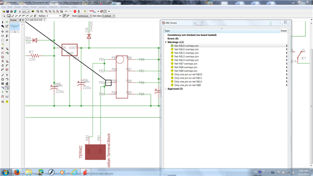
    Thank you Alfred, however, the advice you gave did not help. I tried to both realign the schematic and symbol separately. Each process completed but stated that nothing was done. I am attaching a picture for you to see the areas that are in question. Is there anything else I can do?

    Thanks again!


    image

    • Cancel
    • Vote Up 0 Vote Down
    • Sign in to reply
    • Cancel
  • e14 Contributor
    e14 Contributor over 12 years ago in reply to e14 Contributor

    I resolved the issue by redrawing the devices I made and redrawing the schematic from scratch while importing the new devices. Something was stuck on a metric grid apparently. Thanks for your response. :-)


    Can you point me to a resource for designing copper planes in eagle - a tutorial if you will on power/gnd plane construction?


    Thanks in advance!

    • Cancel
    • Vote Up 0 Vote Down
    • Sign in to reply
    • Cancel
  • e14 Contributor
    e14 Contributor over 12 years ago in reply to e14 Contributor

    Am 22.05.2014 14:04, schrieb J Chop:

    Thank you Alfred, however, the advice you gave did not help. I tried to

    both realign the schematic and symbol separately. Each process completed

    but stated that nothing was done. I am attaching a picture for you to

    see the areas that are in question. Is there anything else I can do?

    Thanks again!


    1. please check the coordinate of the PIN in SYMBOL, must be 0.1 inch

        grid.

    2. check the Gate in device-editor, must be in 0.1 inch grid.


    3. check the origin of the gates in schematic, must be in 0.1 inch grid.


    Do you have run the ULPs in exact order:

    RUN snap-pin-in-symbol (Symbol-Editor)

    UPDATE library  (Schematic Editor)

    RUN snap-on-grid-sch.ulp (Schematic Editor)


    How do you draw the net? By NET-Command, or WIRE-Commend?


    For more support, you can send me the schematic.


    ***

    Um das Original zu lesen, und auch zuverlässig angehängte Dateien

    bereitstellen zu können, benutzen Sie news.cadsoft.de und einen

    funktionierenden News-Reader wie Thunderbird!

    ***


    Mit freundlichen Grüßen / Best regards


    Alfred Zaffran

    --

    ______________________________________________________________

    Alfred Zaffran              Support

    CadSoft Computer GmbH       Hotline:   08635-698930

    Pleidolfweg 15              FAX:       08635-698940

    84568 Pleiskirchen          eMail: <alf@cadsoft.de>

                                 Web:   <www.cadsoft.de>

    Registergericht: Amtsgericht Traunstein HRB 5573

    Geschäftsführer: Thomas Liratsch

    ______________________________________________________________

    EAGLE V6.5 availabe now!


    • Cancel
    • Vote Up 0 Vote Down
    • Sign in to reply
    • Cancel
  • e14 Contributor
    e14 Contributor over 12 years ago in reply to e14 Contributor

    I resolved the issue by redrawing the devices I made and redrawing the schematic from scratch while importing the new devices. Something was stuck on a metric grid apparently. Thanks for your response. :-)


    Can you point me to a resource for designing copper planes in eagle - a tutorial if you will on power/gnd plane construction?


    Thanks in advance!

    • Cancel
    • Vote Up 0 Vote Down
    • Sign in to reply
    • Cancel
Reply
  • e14 Contributor
    e14 Contributor over 12 years ago in reply to e14 Contributor

    I resolved the issue by redrawing the devices I made and redrawing the schematic from scratch while importing the new devices. Something was stuck on a metric grid apparently. Thanks for your response. :-)


    Can you point me to a resource for designing copper planes in eagle - a tutorial if you will on power/gnd plane construction?


    Thanks in advance!

    • Cancel
    • Vote Up 0 Vote Down
    • Sign in to reply
    • Cancel
Children
No Data
element14 Community

element14 is the first online community specifically for engineers. Connect with your peers and get expert answers to your questions.

  • Members
  • Learn
  • Technologies
  • Challenges & Projects
  • Products
  • Store
  • About Us
  • Feedback & Support
  • FAQs
  • Terms of Use
  • Privacy Policy
  • Legal and Copyright Notices
  • Sitemap
  • Cookies

An Avnet Company © 2026 Premier Farnell Limited. All Rights Reserved.

Premier Farnell Ltd, registered in England and Wales (no 00876412), registered office: Farnell House, Forge Lane, Leeds LS12 2NE.

Follow element14

  • X
  • Facebook
  • linkedin
  • YouTube