I need to design a two layered PCB as shown below. How can I define the two layers. Thanks
Use layer 1 and 16 in Eagle, eg. layer setup would be "(1*16)", and create your board.
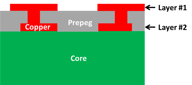
Tell your pcb manufacturer to use the following layer stack-up:
* silkscreen
* soldermask
* layer 1
* prepreg
* layer 16
* core
If what you call core is really a core not aluminum, else you'd add an insulation layer between layer 16 and core.
Thanks for the reply. That was very useful.
I have a follow up question. How can I define a blind via in Eagle with layer configuration (1*16)? Should I just create through Vias and let the PCB manufacturer know that they have to stop on layer 16?
In addition to the layer stack-up let him know that vias are only between layer 1 and 16 (or 2 from his point of view).
I've also found this page for you: "How to design PCB stackup - (FEDEVEL)"
Thanks