


Hello
I am a new user for Eagle and trying to learn from the Basic.
This may not be a big problem but it bothers me a lot.
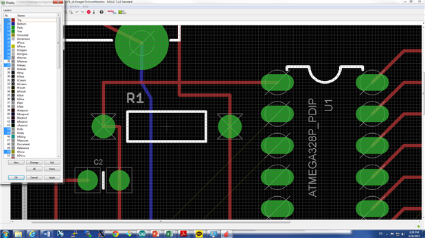
So basically, I cannot see the drill of Via on Layout editor. I attached pictures

The right one is layout practice example from Sparkfun site. I tried to draw the same thing but as you see there is no holes and just filled pads shown on my layout editors.
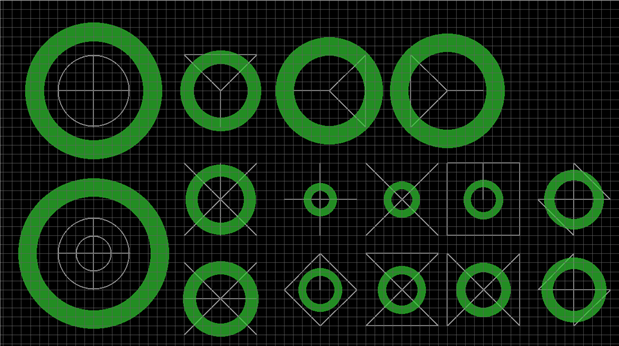
If I checked 44 Drill on Display it just show the stupid lines on the pads sometime X sometimes Square or just line....
Can anybody help me to figure out this?
The thing is.. I don't know whether it is Via with through-hole or just a pad for the electronic component... It is really annoying..
Please help me~!


