Hello,
I am very new to Eagle so please bare with me! I am very confused as to what I have created is ‘correct’ in any way, so my main question is - Does this look right to you?
I am creating a very simple Arduino Nano-based device and hope to create a combination of a breadboard and a routed PCB so that you can easily ‘plug in’ and solder the modules to the board. Much like the ‘build your own’ kits that you can find from Sparkfun etc.
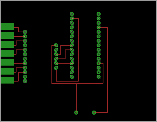
The board consists of module (the MPR121) that needs to be attached to some larger electrodes on the PCB. I have been experimenting with using the plated shapes at the edge of my prototyping breadboard (image below) which work well, but there isn’t a way of connecting them efficiently. So - the routed part contains "only" the connection between the drilled pads on the edge of the PCB to a number of plated holes on the breadboard.
I have attached a picture of my current sketch. The green layer consists of drilled solder pads for the components, and the electrodes demonstrated on the left hand side just need to be copper. The holes will be drilled like a normal breadboard, and the red lines are the traces between the pins.
The pitch is 0.1 inches, hole sizes are 2.15mm in diameter and the inner hole to be drilled is 1mm.
The overall board will be 3.5 by 2.7 inches, and the design will go to one edge to leave room on the blank board at the other edge.
Thank you so so much