element14 Community
element14 Community
    Register Log In
  • Site
  • Search
  • Log In Register
  • Community Hub
    Community Hub
    • What's New on element14
    • Feedback and Support
    • Benefits of Membership
    • Personal Blogs
    • Members Area
    • Achievement Levels
  • Learn
    Learn
    • Ask an Expert
    • eBooks
    • element14 presents
    • Learning Center
    • Tech Spotlight
    • STEM Academy
    • Webinars, Training and Events
    • Learning Groups
  • Technologies
    Technologies
    • 3D Printing
    • FPGA
    • Industrial Automation
    • Internet of Things
    • Power & Energy
    • Sensors
    • Technology Groups
  • Challenges & Projects
    Challenges & Projects
    • Design Challenges
    • element14 presents Projects
    • Project14
    • Arduino Projects
    • Raspberry Pi Projects
    • Project Groups
  • Products
    Products
    • Arduino
    • Avnet & Tria Boards Community
    • Dev Tools
    • Manufacturers
    • Multicomp Pro
    • Product Groups
    • Raspberry Pi
    • RoadTests & Reviews
  • About Us
    About the element14 Community
  • Store
    Store
    • Visit Your Store
    • Choose another store...
      • Europe
      •  Austria (German)
      •  Belgium (Dutch, French)
      •  Bulgaria (Bulgarian)
      •  Czech Republic (Czech)
      •  Denmark (Danish)
      •  Estonia (Estonian)
      •  Finland (Finnish)
      •  France (French)
      •  Germany (German)
      •  Hungary (Hungarian)
      •  Ireland
      •  Israel
      •  Italy (Italian)
      •  Latvia (Latvian)
      •  
      •  Lithuania (Lithuanian)
      •  Netherlands (Dutch)
      •  Norway (Norwegian)
      •  Poland (Polish)
      •  Portugal (Portuguese)
      •  Romania (Romanian)
      •  Russia (Russian)
      •  Slovakia (Slovak)
      •  Slovenia (Slovenian)
      •  Spain (Spanish)
      •  Sweden (Swedish)
      •  Switzerland(German, French)
      •  Turkey (Turkish)
      •  United Kingdom
      • Asia Pacific
      •  Australia
      •  China
      •  Hong Kong
      •  India
      •  Japan
      •  Korea (Korean)
      •  Malaysia
      •  New Zealand
      •  Philippines
      •  Singapore
      •  Taiwan
      •  Thailand (Thai)
      •  Vietnam
      • Americas
      •  Brazil (Portuguese)
      •  Canada
      •  Mexico (Spanish)
      •  United States
      Can't find the country/region you're looking for? Visit our export site or find a local distributor.
  • Translate
  • Profile
  • Settings
Autodesk EAGLE
  • Products
  • More
Autodesk EAGLE
EAGLE User Support (English) Seems I've put a dimension on the top copper layer
  • Blog
  • Forum
  • Documents
  • Events
  • Polls
  • Files
  • Members
  • Mentions
  • Sub-Groups
  • Tags
  • More
  • Cancel
  • New
Join Autodesk EAGLE to participate - click to join for free!
Actions
  • Share
  • More
  • Cancel
Forum Thread Details
  • State Verified Answer
  • Replies 10 replies
  • Subscribers 188 subscribers
  • Views 1166 views
  • Users 0 members are here
Related

Seems I've put a dimension on the top copper layer

e14 Contributor
e14 Contributor over 10 years ago

Hi Forum,

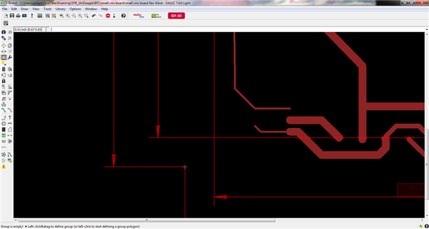
Really new to Eagle, and it seems I've somehow put a dimension (DRAW+DIMENSION) on the top (copper) layer. Now I can't remove it. I've tried ripup and delete but the copper (if that's what it is remains. Can anyone help? The forum package does not allow me to attach the files, so I have attached an image - the dimension was a 2mm spacing check - it is situated just under pins 1 and 2 of the 6 pin JST-PH connector "MOT_IO" - top right of the board.

Any help would be greatly appreciated.

Thanks,

Chris

Attachments:
image
  • Sign in to reply
  • Cancel
  • autodeskguest
    0 autodeskguest over 10 years ago in reply to e14 Contributor

    On 26.05.2016 17:46, Philip Blaze wrote:

    I am having the same problem except that I can not select any part of the remaining dimension as a part, or the whole thing as a group. When I loaded the board from the file, there were dimension values in the hatched boxes, I was able to select and delete those, but what remains looks like some kind of hatched or vectorized line which I can't select in any way or get any information on. On this picture, I'm showing only the top copper layer. Suggestions?


    --

    To view any images and attachments in this post, visit:

    https://www.element14.com/community/message/197969


    It was probably areas marked as errors by the DRC. You can clear it from

    there.


    • Cancel
    • Vote Up 0 Vote Down
    • Sign in to reply
    • Verify Answer
    • Cancel
  • autodeskguest
    0 autodeskguest over 10 years ago in reply to e14 Contributor

    On 26.05.2016 17:46, Philip Blaze wrote:

    I am having the same problem except that I can not select any part of the remaining dimension as a part, or the whole thing as a group. When I loaded the board from the file, there were dimension values in the hatched boxes, I was able to select and delete those, but what remains looks like some kind of hatched or vectorized line which I can't select in any way or get any information on. On this picture, I'm showing only the top copper layer. Suggestions?


    --

    To view any images and attachments in this post, visit:

    https://www.element14.com/community/message/197969


    It was probably areas marked as errors by the DRC. You can clear it from

    there.


    • Cancel
    • Vote Up 0 Vote Down
    • Sign in to reply
    • Verify Answer
    • Cancel
  • e14 Contributor
    0 e14 Contributor over 10 years ago in reply to e14 Contributor

    Crap. Never mind. It was an artifact. I would suggest this be added to the bug list.

    • Cancel
    • Vote Up 0 Vote Down
    • Sign in to reply
    • Verify Answer
    • Cancel
  • e14 Contributor
    0 e14 Contributor over 10 years ago

    I am having the same problem except that I can not select any part of the remaining dimension as a part, or the whole thing as a group. When I loaded the board from the file, there were dimension values in the hatched boxes, I was able to select and delete those, but what remains looks like some kind of hatched or vectorized line which I can't select in any way or get any information on. On this picture, I'm showing only the top copper layer. Suggestions?image

    • Cancel
    • Vote Up 0 Vote Down
    • Sign in to reply
    • Verify Answer
    • Cancel
  • shabaz
    0 shabaz over 10 years ago in reply to e14 Contributor

    No worries, glad it is all sorted : )

    • Cancel
    • Vote Up 0 Vote Down
    • Sign in to reply
    • Verify Answer
    • Cancel
  • e14 Contributor
    0 e14 Contributor over 10 years ago in reply to e14 Contributor

    OK - maybe a little hasty to post this as I have found the answer. I used the layer settings to remove all except the top layer, zoomed in and selected the MOVE command, I then clicked around the dimension until it was highlighted, extended it off the board and deleted it. Thans so much to shabaz - and sorry to have wasted your time my friend.

    Best wishes,

    Chris

    • Cancel
    • Vote Up 0 Vote Down
    • Sign in to reply
    • Verify Answer
    • Cancel
  • shabaz
    0 shabaz over 10 years ago in reply to e14 Contributor

    I'm afraid I cannot see what could cause this : (

    What happens if you click the dashed box icon, and then drag to select a group, does it become brighter red than the stuff that wasn't selected?

    I've tried creating a dimension on my copy of EAGLE, but I can delete it using the usual delete icon (the one that looks like an 'X').

    Selecting a group of parts does make it become bright red, which in my case means it should be deletable too.

    If in your case it becomes bright too, then that usually means it is deletable but that something else is being selected when you click near it.

    Also, If you select Info (the 'i' icon), does it display any information when you click on the dimension?

    • Cancel
    • Vote Up +1 Vote Down
    • Sign in to reply
    • Reject Answer
    • Cancel
  • e14 Contributor
    0 e14 Contributor over 10 years ago in reply to e14 Contributor

    Just as a point - I did add the dimension to confirm the pitch of the connector, so I don't think it could be part of the component library - I think I just added the dimension and it somehow has become printed in copper on the top layer.

    • Cancel
    • Vote Up 0 Vote Down
    • Sign in to reply
    • Verify Answer
    • Cancel
  • e14 Contributor
    0 e14 Contributor over 10 years ago in reply to shabaz

    Hi Shabaz, the only component it is associated with is the JST connector - and I have used that a lot on other boards without the dimension being added, Is that what you mean - or that the dimension marking is somehow a component  in its own right?

    Thanks for the REALLY rapid response

    • Cancel
    • Vote Up 0 Vote Down
    • Sign in to reply
    • Verify Answer
    • Cancel
  • shabaz
    0 shabaz over 10 years ago

    Hi Chris,


    Is it something perhaps that might have been done during library component creation?

    If so, then it needs to be deleted from the library (it is not possible to delete it from the PCB layout if

    this was drawn in the package in the library).

    • Cancel
    • Vote Up 0 Vote Down
    • Sign in to reply
    • Verify Answer
    • Cancel
element14 Community

element14 is the first online community specifically for engineers. Connect with your peers and get expert answers to your questions.

  • Members
  • Learn
  • Technologies
  • Challenges & Projects
  • Products
  • Store
  • About Us
  • Feedback & Support
  • FAQs
  • Terms of Use
  • Privacy Policy
  • Legal and Copyright Notices
  • Sitemap
  • Cookies

An Avnet Company © 2026 Premier Farnell Limited. All Rights Reserved.

Premier Farnell Ltd, registered in England and Wales (no 00876412), registered office: Farnell House, Forge Lane, Leeds LS12 2NE.

Follow element14

  • X
  • Facebook
  • linkedin
  • YouTube