


Hi,
I'm trying to create a package that has an exposed thermal pad with multiple connections to the bottom layer part of the thermal pad. I have searched various forums and I still do not see how to do it. Most answers to this question, or similar, talk about placing vias on top of an SMD pad. However, when designing a package, you cannot place vias - only through-hole pads.
I have tried using SMD pads, poured polygons and rectangles as the base copper and placed TH pads on top and I always get some form of overlap error from DRC.
Here is an example of a PDSO-10 package and the result of running DRC. This particular example uses an SMD pad as the base with 5 TH pads on top. As you can see, I get 5 overlap errors. If I replace the SMD base pad with a poured polygon or a rectangle, I also get overlap errors. The overlap errors are due to the copper, not any other layer such as tStop or tCream. I have determined that fact by selectively hiding layers and testing if the overlap errors go away.

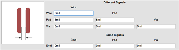
In the package design I have named the SMD pad and the TH pads EP@1, EP@2, etc. etc. In the Symbol design, I have a pin named EP. Eagle version is 6.5. My design rules are:
Any ideas?
Kind regards,
AC


