element14 Community
element14 Community
    Register Log In
  • Site
  • Search
  • Log In Register
  • Community Hub
    Community Hub
    • What's New on element14
    • Feedback and Support
    • Benefits of Membership
    • Personal Blogs
    • Members Area
    • Achievement Levels
  • Learn
    Learn
    • Ask an Expert
    • eBooks
    • element14 presents
    • Learning Center
    • Tech Spotlight
    • STEM Academy
    • Webinars, Training and Events
    • Learning Groups
  • Technologies
    Technologies
    • 3D Printing
    • FPGA
    • Industrial Automation
    • Internet of Things
    • Power & Energy
    • Sensors
    • Technology Groups
  • Challenges & Projects
    Challenges & Projects
    • Design Challenges
    • element14 presents Projects
    • Project14
    • Arduino Projects
    • Raspberry Pi Projects
    • Project Groups
  • Products
    Products
    • Arduino
    • Avnet & Tria Boards Community
    • Dev Tools
    • Manufacturers
    • Multicomp Pro
    • Product Groups
    • Raspberry Pi
    • RoadTests & Reviews
  • About Us
  • Store
    Store
    • Visit Your Store
    • Choose another store...
      • Europe
      •  Austria (German)
      •  Belgium (Dutch, French)
      •  Bulgaria (Bulgarian)
      •  Czech Republic (Czech)
      •  Denmark (Danish)
      •  Estonia (Estonian)
      •  Finland (Finnish)
      •  France (French)
      •  Germany (German)
      •  Hungary (Hungarian)
      •  Ireland
      •  Israel
      •  Italy (Italian)
      •  Latvia (Latvian)
      •  
      •  Lithuania (Lithuanian)
      •  Netherlands (Dutch)
      •  Norway (Norwegian)
      •  Poland (Polish)
      •  Portugal (Portuguese)
      •  Romania (Romanian)
      •  Russia (Russian)
      •  Slovakia (Slovak)
      •  Slovenia (Slovenian)
      •  Spain (Spanish)
      •  Sweden (Swedish)
      •  Switzerland(German, French)
      •  Turkey (Turkish)
      •  United Kingdom
      • Asia Pacific
      •  Australia
      •  China
      •  Hong Kong
      •  India
      • Japan
      •  Korea (Korean)
      •  Malaysia
      •  New Zealand
      •  Philippines
      •  Singapore
      •  Taiwan
      •  Thailand (Thai)
      • Vietnam
      • Americas
      •  Brazil (Portuguese)
      •  Canada
      •  Mexico (Spanish)
      •  United States
      Can't find the country/region you're looking for? Visit our export site or find a local distributor.
  • Translate
  • Profile
  • Settings
Autodesk EAGLE
  • Products
  • More
Autodesk EAGLE
EAGLE User Support (English) LT3759 exposed Pad
  • Blog
  • Forum
  • Documents
  • Events
  • Polls
  • Files
  • Members
  • Mentions
  • Sub-Groups
  • Tags
  • More
  • Cancel
  • New
Join Autodesk EAGLE to participate - click to join for free!
Actions
  • Share
  • More
  • Cancel
Forum Thread Details
  • State Suggested Answer
  • Replies 14 replies
  • Answers 1 answer
  • Subscribers 180 subscribers
  • Views 1935 views
  • Users 0 members are here
Related

LT3759 exposed Pad

nikoly
nikoly over 9 years ago

I'm using a 2 Layer Board in Eagle .

The datasheet gives some info about the layout, advising me to add some  vias inside that Pad for heatsink problems.

I have opened Eagle tutorial "ti-launchpad" where there are  2 IC with Pads and vias on them (how in the image)p .image

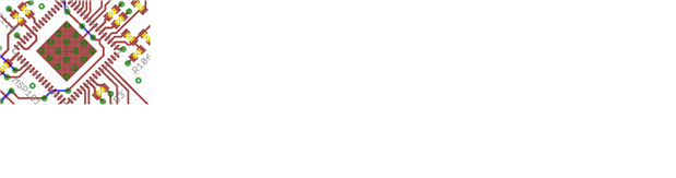
Watching the DRC I have some overlap errors.

I can follow that way in order to design my board but I wonder if it's the right way to do this or not !

I have also seen someone to put arrays of pads instead of vias in order to get this!


Hope you can put me in the right direction!

Thanks a lot

Nico

  • Sign in to reply
  • Cancel
Parents
  • rachaelp
    0 rachaelp over 9 years ago

    Hi Nico,


    I've seen people say all sorts of things about the way to deal with this but to be honest just placing vias in the pad and approving all the resulting DRC errors seems the simplest way forward to me and I have done it this way plenty of times without issue. The only problem is if you move the IC and vias the DRC approvals need to be done again.


    When placing vias in the pad like this you do need to be careful of the drill size. If the via is too large then the solder will get wicked away from under the IC when it's reflowed. With more complicated boards you can use a combination if microvias and buried vias to eliminate the solder wicking away problem but for standard boards with just through vias then just make sure the drill size for this is small enough to reduce the risk.


    I think usually they are expecting that these devices are placed on multi layer boards with a solid 0V plane which doubles as a heat sink to take the heat away into the surrounding board. With a 2-layer board you wont have as much heat dissipation from this method so you might need to keep an eye on the device temperature when getting your board up and running. Also be aware that when building boards like this then the manufacturer who is assembling your board needs to know there are heatsink structures on these thermal pads so they can adjust their temperature profiles to ensure enough heat gets into the board so the thermal pad reflows properly.


    Best Regards,


    Rachael

    • Cancel
    • Vote Up 0 Vote Down
    • Sign in to reply
    • Verify Answer
    • Cancel
Reply
  • rachaelp
    0 rachaelp over 9 years ago

    Hi Nico,


    I've seen people say all sorts of things about the way to deal with this but to be honest just placing vias in the pad and approving all the resulting DRC errors seems the simplest way forward to me and I have done it this way plenty of times without issue. The only problem is if you move the IC and vias the DRC approvals need to be done again.


    When placing vias in the pad like this you do need to be careful of the drill size. If the via is too large then the solder will get wicked away from under the IC when it's reflowed. With more complicated boards you can use a combination if microvias and buried vias to eliminate the solder wicking away problem but for standard boards with just through vias then just make sure the drill size for this is small enough to reduce the risk.


    I think usually they are expecting that these devices are placed on multi layer boards with a solid 0V plane which doubles as a heat sink to take the heat away into the surrounding board. With a 2-layer board you wont have as much heat dissipation from this method so you might need to keep an eye on the device temperature when getting your board up and running. Also be aware that when building boards like this then the manufacturer who is assembling your board needs to know there are heatsink structures on these thermal pads so they can adjust their temperature profiles to ensure enough heat gets into the board so the thermal pad reflows properly.


    Best Regards,


    Rachael

    • Cancel
    • Vote Up 0 Vote Down
    • Sign in to reply
    • Verify Answer
    • Cancel
Children
  • nikoly
    0 nikoly over 9 years ago in reply to rachaelp

    Hi Rachael ,

    thanks for the reply.

    I 've also immagined that this kind of IC requires a minimum 4 layers board in order to benefit from the exposed pad presence but since its the first time I needed an advice on this issue.


    Reading this tutorial (http://www.ti.com/lit/an/slma002g/slma002g.pdf ) from texas (see also the attached image) it seems that in a 1 or 2 layer board I can use the top layer for heatSink problem.

    In addition it confirms what you said about using the 4 or more board layers board and buried vias.


    So if I decide to use the 2 layer approach I should create a copper polygon as big as possible (the red figure in the attched image)  but I cant understand where (in the package editor) or in the layout board!

    Do you have any advice on how to realize this ?image


    Thanks again for the support!

    Nico

    • Cancel
    • Vote Up 0 Vote Down
    • Sign in to reply
    • Verify Answer
    • Cancel
  • rachaelp
    0 rachaelp over 9 years ago in reply to nikoly

    Hi Nico,


    So in the package editor as part of the library part you need to create the thermal pad the correct recommended size for the part, this will ensure the solderable area on the pad a) doesn't have solder resist and b) is the correct size so that when it reflows it centres the part correctly otherwise your part can end up moving off your pads and not sitting correctly. Usually these thermal pads are connected to your 0V rail in your system, it usually tells you in the datasheet if it's to be connected to the same 0V reference as the 0V pins. You should put a pin on your symbol to represent the thermal pad and connect it to your system 0V if this is indeed the case.


    Then in the schematic you would draw a polygon on the top layer (assuming it placed on the top of the board) around the pad and extending along the board to wherever you wanted it to be. You then name this polygon to 0V (or whatever you called your 0V reference) and it would connect to your thermal pad. You'll probably want to turn the thermal relief off (uncheck Thermals) in the polygon properties.


    Let me know if you need any more help.


    Best Regards,


    Rachael

    • Cancel
    • Vote Up 0 Vote Down
    • Sign in to reply
    • Verify Answer
    • Cancel
element14 Community

element14 is the first online community specifically for engineers. Connect with your peers and get expert answers to your questions.

  • Members
  • Learn
  • Technologies
  • Challenges & Projects
  • Products
  • Store
  • About Us
  • Feedback & Support
  • FAQs
  • Terms of Use
  • Privacy Policy
  • Legal and Copyright Notices
  • Sitemap
  • Cookies

An Avnet Company © 2026 Premier Farnell Limited. All Rights Reserved.

Premier Farnell Ltd, registered in England and Wales (no 00876412), registered office: Farnell House, Forge Lane, Leeds LS12 2NE.

ICP 备案号 10220084.

Follow element14

  • X
  • Facebook
  • linkedin
  • YouTube