Evening all
Anybody got a library for a texas inst OPA569 ?
http://www.ti.com/general/docs/lit/getliterature.tsp?genericPartNumber=opa569&fileType=pdf
had a go making it myself but struggling with the heat pad and via's
Steve
Evening all
Anybody got a library for a texas inst OPA569 ?
http://www.ti.com/general/docs/lit/getliterature.tsp?genericPartNumber=opa569&fileType=pdf
had a go making it myself but struggling with the heat pad and via's
Steve
Am 08.06.2016 um 22:32 schrieb stephen clarke:
Evening all
Anybody got a library for a texas inst OPA569 ?
http://www.ti.com/general/docs/lit/getliterature.tsp?genericPartNumber=opa569&fileType=pdf
had a go making it myself but struggling with the heat pad and via's
Steve
--
To view any images and attachments in this post, visit:
https://www.element14.com/community/message/199039
Why don't you place here what you have done already so we can help you?
--
Mit freundlichen Grüßen / With best regards
Joern Paschedag
Am 08.06.2016 um 22:32 schrieb stephen clarke:
Evening all
Anybody got a library for a texas inst OPA569 ?
http://www.ti.com/general/docs/lit/getliterature.tsp?genericPartNumber=opa569&fileType=pdf
had a go making it myself but struggling with the heat pad and via's
Steve
--
To view any images and attachments in this post, visit:
https://www.element14.com/community/message/199039
Why don't you place here what you have done already so we can help you?
--
Mit freundlichen Grüßen / With best regards
Joern Paschedag
thank you for the response
Sorry i have been busy at work
i am struggling a bit with the following
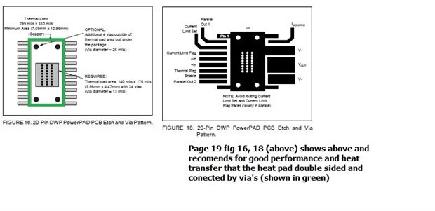
Page 19 fig 16 and 18 shows the recommended pcb layout.
Fig 16 shows that a thermal pad should be under the ic (highlighted in green) with a exposed area for contact with the ic pad, it further states that it is recommended that this pad is double sided and connected by via's. the via sizes are given this is for wicking on the solder process. there should be another 4 in the corners i presume this is for thermal bonding of the two copper area's this pad should be connected to pins 1,10,11,20.
I am not sure on how to go about this going to have another go this weekend.
i am also unsure of how to go about the connections for the following pins as the above fig 18 shows large copper area's
Pins 12,13 V+
Pins 14,15 Output
Pins 17,18 V-
Thank you
Steve