


Hi All,
I am fairly new to eagle. I am hoping to get some advise on a beginners problem that I am facing.
I am designing a board which should just contain a bunch of holes for 0.1" breakway header pins to be connected and traces to connect different terminals.
When I try to visualize my gerber files, they appear to be solid pads, with no holes.
For example a part of board looks like this:

But when I look at the gerber files (GTL), through circuitpeople.com, I see this:
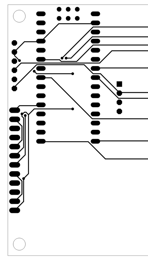
Clearly, there are no holes in here, it looks like they are all just pads!!
Do I have to manually put holes in each pad?
Thanks in advance,
Souvik.