


Hello,
I am trying to make a 4-layer pcb with the following layers: TOP, BOTTOM, GND, and VCC. I made GND and VCC layers, and made polygons covering the GND and VCC layers that are assigned to each respective layer and named GND and VCC respectively (See the FIG 1 & 2). However when I use autorouter, it is evident that the components on my board are not connecting to the VCC layer. The first image shows a top layer image with VCC lines routed across the surface. Shouldn't the components just connect to the VCC layer directly by passing through to that layer on the board directly?
Thank you in advance for your help!

FIGURE 1

FIGURE 2

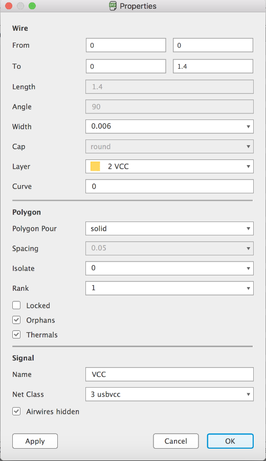
FIGURE 3


