Good evening,
I am breaking my head on a clearance error in Eagle.
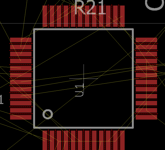
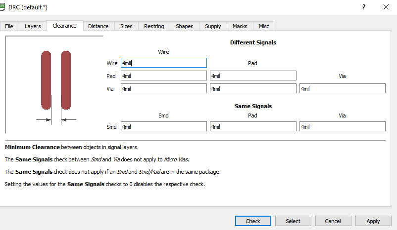
The W5500 gives me clearance errors between all pads, while the distance between the pads is well within the allowed pad-distance of the DRC. distance between pads is 7.9mm.
I tried all settings but it seems like this problem is within the component itself. any suggestions what I could do about it?
Much appreciated!