Hello all, I am having a 2 layer PCB manufactured by a fab shop. The PCB was designed in Eagle but I am having a problem I haven't encountered before.
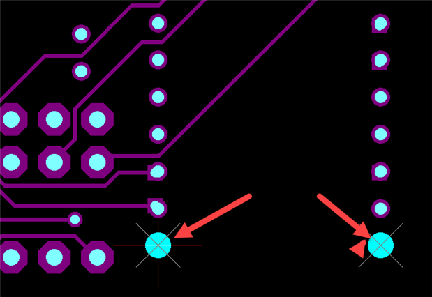
I sent in my GERBER files and they responded by saying there are no copper pads on the bottom layer, only on the top layer. It was my understanding all through holes are PTH (plated all the way through). I checked on older PCBs I have sent in and the through hole devices are the same. They're saying I need to make a separate set of through holes on the bottom layer that line up with the top layer. Previous boards I have made with this fab shop, using the same through hole device, were plated all the way through, I did not need to make a second set of aligned holes. I am at a loss of what is missing for them? is there a setting in Eagle that only allows plating through a certain thickness of PCB or something?
I have searched around, made some adjustments, but I keep getting the same answer back from the shop. My silkscreen/soldermask bottom and top layers are not covering the pads top and bottom either as far as I can tell, can anyone see anything that sticks out at them?
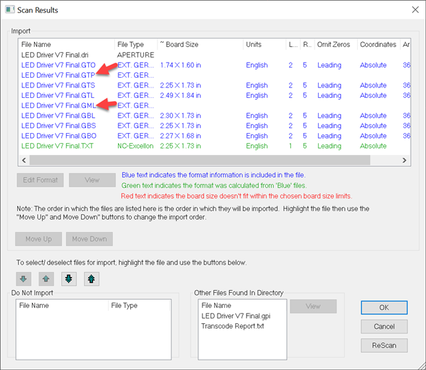
The GERBER files I sent in are attached and have all layers top and bottom.