Hi,
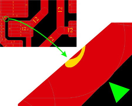
I have set DRC rules for minimum width and clearance to 5 mils. Everything is perfectly fine in the board editor, but when gerbers are generated using the CAM processor, there are some spots with clearance less than 5 mils. For example, a clearance between a top layer rounded SMD pad and ground polygon goes down to 4.85 mils (marked by white marks in the attached image). The problem was detected by the board house because it violated their DRC. I don't have a gerber viewer that would support the DRC, but the problem can also be verified bya measuring tool. Any idea what to do about this?
Thanks.
Attachments:
 |