Hi
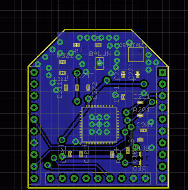
hope this is the right place for getting feedback on my first desgin
it should be bee board http://www.seeedstudio.com/wiki/Bluetooth_Bee with TI cc2540/cc2541 bluetooth low energy MCU http://www.ti.com/product/cc2540&DCMP=LowPowerRFICs+Other&HQS=Other+OT+cc2540
I probably made design mistakes and will be glade to hear from you
first, this is small board so used
1) 8mil data track size, 10-16 mil GND and VCC track size
2) 8mil clearance
3) 8mil distance
3) 20mil drill
can really batchPcb handle it? (the site say yes)
some specific questions
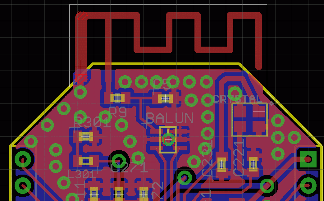
up area
1) I design the PCB antenna from spec http://www.ti.com/lit/an/swra117d/swra117d.pdf
DRC return overlap error of some antenna parts, corner and connection
way? what to do with it?
2) balun part http://www.ti.com/lit/an/swra380a/swra380a.pdf
this part probably need via under (can be found in TI usb BLE desgin http://www.ti.com/lit/ug/swru270b/swru270b.pdf) , as you can see the 20 mil via is little bit big
and over three pads all ground.
DRC return overlap and clearance errors, can I ignore it as it is overlap ground pads?
what else can I do?
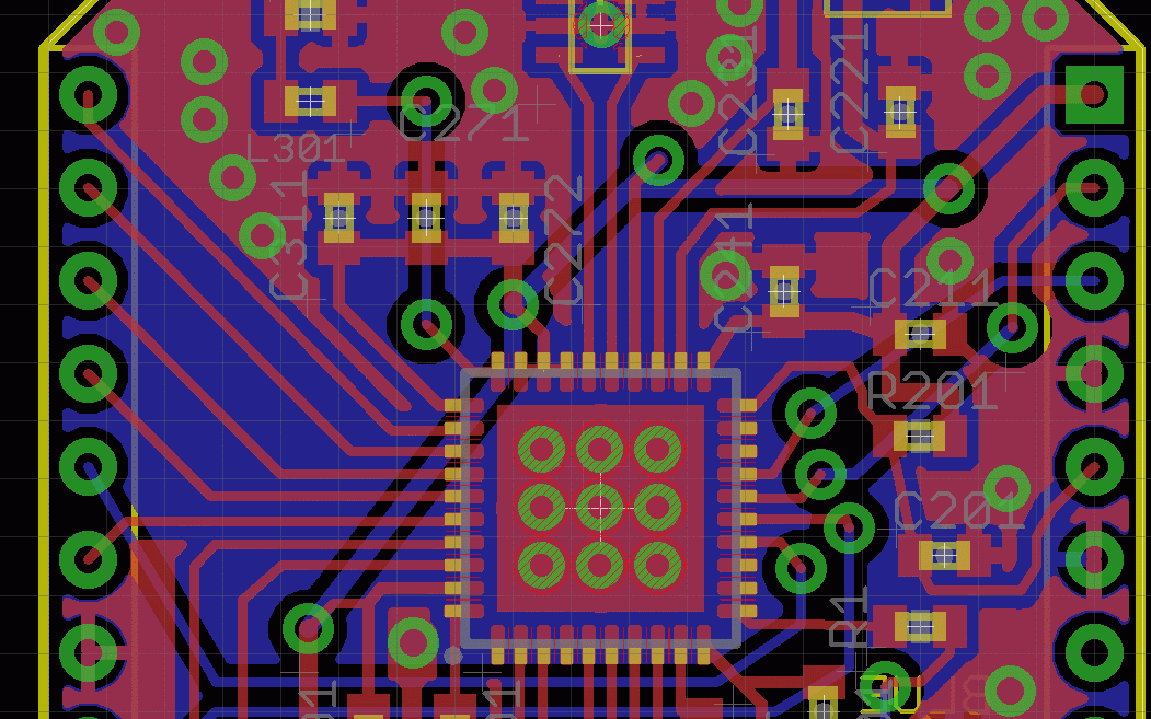
center area
1) the MCU part (which I did not design)
DRC return overlap and clearance errors for all its pads, can I ignore it as this are the MCU dimensions?
2) MCU should have via under is ground plate as in the picture
DRC return overlap what should I do?
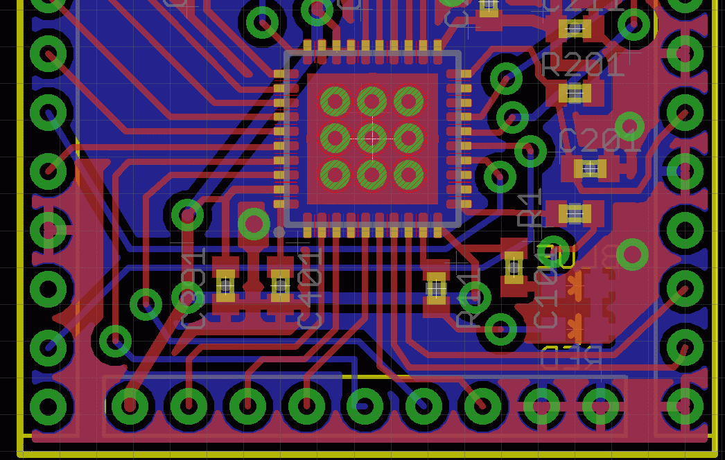
other
1) my GND and VCC route are 10-16 mil instead of 8 mil, is it better?
2) not all my route are 45deg because of space issues, is it critical?
3) I have made some route T junctions,are they ok?
thanks


