element14 Community
element14 Community
    Register Log In
  • Site
  • Search
  • Log In Register
  • Members
    Members
    • Achievement Levels
    • Benefits of Membership
    • Feedback and Support
    • Members Area
    • Personal Blogs
    • What's New on element14
  • Learn
    Learn
    • eBooks
    • Learning Center
    • Learning Groups
    • STEM Academy
    • Webinars, Training and Events
  • Technologies
    Technologies
    • 3D Printing
    • Experts & Guidance
    • FPGA
    • Industrial Automation
    • Internet of Things
    • Power & Energy
    • Sensors
    • Technology Groups
  • Challenges & Projects
    Challenges & Projects
    • Arduino Projects
    • Design Challenges
    • element14 presents
    • Project14
    • Project Groups
    • Raspberry Pi Projects
  • Products
    Products
    • Arduino
    • Avnet Boards Community
    • Dev Tools
    • Manufacturers
    • Product Groups
    • Raspberry Pi
    • RoadTests & Reviews
  • Store
    Store
    • Visit Your Store
    • 'Choose another store...'
      • Europe
      •  Austria (German)
      •  Belgium (Dutch, French)
      •  Bulgaria (Bulgarian)
      •  Czech Republic (Czech)
      •  Denmark (Danish)
      •  Estonia (Estonian)
      •  Finland (Finnish)
      •  France (French)
      •  Germany (German)
      •  Hungary (Hungarian)
      •  Ireland
      •  Israel
      •  Italy (Italian)
      •  Latvia (Latvian)
      •  
      •  Lithuania (Lithuanian)
      •  Netherlands (Dutch)
      •  Norway (Norwegian)
      •  Poland (Polish)
      •  Portugal (Portuguese)
      •  Romania (Romanian)
      •  Russia (Russian)
      •  Slovakia (Slovak)
      •  Slovenia (Slovenian)
      •  Spain (Spanish)
      •  Sweden (Swedish)
      •  Switzerland(German, French)
      •  Turkey (Turkish)
      •  United Kingdom
      • Asia Pacific
      •  Australia
      •  China
      •  Hong Kong
      •  India
      •  Korea (Korean)
      •  Malaysia
      •  New Zealand
      •  Philippines
      •  Singapore
      •  Taiwan
      •  Thailand (Thai)
      • Americas
      •  Brazil (Portuguese)
      •  Canada
      •  Mexico (Spanish)
      •  United States
      Can't find the country/region you're looking for? Visit our export site or find a local distributor.
  • Translate
  • Profile
Autodesk EAGLE
  • Products
  • More
Autodesk EAGLE
EAGLE User Support (English) Domepad eagle lib part
  • Blog
  • Forum
  • Documents
  • Events
  • Polls
  • Files
  • Members
  • Mentions
  • Sub-Groups
  • Tags
  • More
  • Cancel
  • New
Autodesk EAGLE requires membership for participation - click to join
Actions
  • Share
  • More
  • Cancel
Forum Thread Details
  • State Not Answered
  • Replies 4 replies
  • Subscribers 145 subscribers
  • Views 147 views
  • Users 0 members are here
  • domepad
  • dome_pad
  • library_part
Related

Domepad eagle lib part

Former Member
Former Member over 10 years ago

image

Hi,


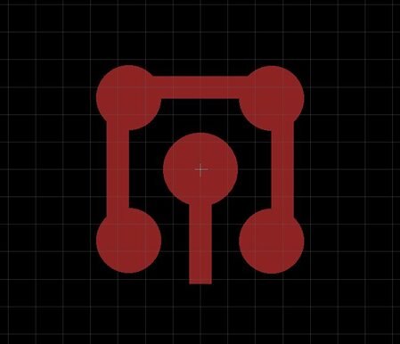
The image above is a so called "domepad", a landing pattern for a button.

But does anybody know how to make this correct in a eagle library element?


The inner part and outside line should be functioning as different pin's.


The problem is that i have to draw with copper to get this shape, else i need to use many different pads.

But this way i get endless DRC errors like clearance and overlap.

And i need to choose a central point (The physical pad for in library) where the connection is made.


Does anybody know how to make a element where i have 2 connection points in the schematic and a DRC free footprint?


Thanks in advance,


Bram van Herck

  • Sign in to reply
  • Cancel
  • Former Member
    0 Former Member over 10 years ago

    Have a read of the manual Section 8.14 Arbitrary Pad shapes.

    The manual is in the docs folder of your installation. This will give you

    an understanding of the requirments for arbitrary pads.


    Attached is a rough library of what you are asking for. Revese engineer it

    to understand how its done especially CONNECT where each pin is connected

    to many pads. The first pin pad connection is made with the CONNECT button

    and subsequent ones made with the APPEND button.


    HTH

    Warren

    --

    Web access to CadSoft support forums at www.eaglecentral.ca.  Where the CadSoft EAGLE community meets.


    • Cancel
    • Vote Up 0 Vote Down
    • Sign in to reply
    • Verify Answer
    • Cancel
  • Former Member
    0 Former Member over 10 years ago in reply to Former Member

    Warren Brayshaw wrote:

    Have a read of the manual Section 8.14 Arbitrary Pad shapes.

    The manual is in the docs folder of your installation. This will give

    you an understanding of the requirments for arbitrary pads.


    Attached is a rough library of what you are asking for. Revese

    engineer it to understand how its done especially CONNECT where each

    pin is connected to many pads. The first pin pad connection is made

    with the CONNECT button and subsequent ones made with the APPEND

    button.


    HTH

    Warren

    --

    Web access to CadSoft support forums at www.eaglecentral.ca.  Where

    the CadSoft EAGLE community meets.


    The attachment reached the Cadsoft News Group correctly but not Element14.

    Will that ever be fixed? Drew??


    File is at Eagle Central but it has a problem there. It picked up an

    additional extension (.htm)  filename.lbr.htm so watch out for and remove

    the additional .htm

    http://www.eaglecentral.ca/forums/index.php/m/148806/09b2cb136ce5b922484789d309009220/#msg_148806


    Warren


    --

    Viewed / responded via the newsgroup at

    news.cadsoft.de


    • Cancel
    • Vote Up 0 Vote Down
    • Sign in to reply
    • Verify Answer
    • Cancel
  • Former Member
    0 Former Member over 10 years ago in reply to Former Member

    Hi Warren,


    Thanks for the quick relpy.

    I'm going to dive into the library and attempt to make my own correct one.


    Bram

    • Cancel
    • Vote Up 0 Vote Down
    • Sign in to reply
    • Verify Answer
    • Cancel
  • Former Member
    0 Former Member over 10 years ago in reply to Former Member

    Bram Herck, van wrote:

    Hi Warren,


    Thanks for the quick relpy.

    I'm going to dive into the library and attempt to make my own correct

    one.


    Bram


    You're welcome.

    Note that that library did not address the  tStop and tCream layers.

    You should turn off the cream for the SMD pads and make a area that should

    be clear of solder stop with a shape on the tStop layer


    Warren


    --

    Viewed / responded via the newsgroup at

    news.cadsoft.de


    • Cancel
    • Vote Up 0 Vote Down
    • Sign in to reply
    • Verify Answer
    • Cancel
element14 Community

element14 is the first online community specifically for engineers. Connect with your peers and get expert answers to your questions.

  • Members
  • Learn
  • Technologies
  • Challenges & Projects
  • Products
  • Store
  • About Us
  • Feedback & Support
  • FAQs
  • Terms of Use
  • Privacy Policy
  • Legal and Copyright Notices
  • Sitemap
  • Cookies

An Avnet Company © 2023 Premier Farnell Limited. All Rights Reserved.

Premier Farnell Ltd, registered in England and Wales (no 00876412), registered office: Farnell House, Forge Lane, Leeds LS12 2NE.

ICP 备案号 10220084.

Follow element14

  • X
  • Facebook
  • linkedin
  • YouTube