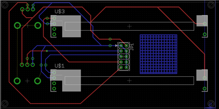
Ok so I just got a issue back from my board house, I combined 5 pcbs in one panel.
You can see the info in the uploaded picture. The plating index is low and it need to bost it up. I understand I need to make the copper distribtion move even (even though im not sure what 'even is') Am I right in saying one way is to add copper traces which dont do anything where I can on the board? Or I read somewhere that you can fill another layer with copper or something like that. Only thing is im working with eagle light so I only have two traces which Ive used both as much as each other on all the boards.
Also where it says it may get brunted for instance where the redish color is on that 10 pin header. That is because I had to ground 4 of the pins, I dont think there is anyway round this as I need to keep it like that. I also attached a zoomed in pic.
Could anyone take a look and tell me what is acctually bad and what needs to be changed. And how I need to go about doing that on eagle.
Thanks!
 | |
 |