Hi guys,
first post.
Let's get right to it.
I'm very inexperienced with Eagle Cad, so it would help to be detailed, don't go overboard though. Hopefully we find a good match.
I'm looking to modify a pre-existing eagle Schematic and board combo to include a 3x2 row of pin headers connected to the microcontroller for easy hookup to do ICSP. I thought it would be great to try this out to improve and get acquainted with Eagle.
For this project, I am ordering a set of 2-row headers.
I took a look at the datasheet for my pin headers. here is a link: http://www.samtec.com/documents/webfiles/pdf/TSW_TH.PDF
I already extracted what I think is the most important information, but let's review so that you can approve. The two pieces of info I took are the thickness of the pin itself, and the distance between 2 pins from their centers.
Pin Thickness: 0.64mm
Distance between center of pins (for all adjacent pins, up/down/left/right): 2.54 mm
I think these are the most essential pieces to have. Please correct me if I'm wrong. Once again, this is my first time doing this.
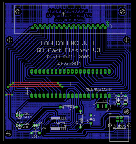
Moving forward, I have some important information that I need to communicate to Eagle. I want to make, and please pardon my language here *symantics, I want to place 2 rows of 3 pin headers connected to the microcontroller as previously stated. Here's a picture of a fabricated circuit that has these pin headers in place:

See at the bottom left of the board.
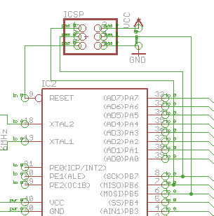
Now, let's take a look at the current image of the board I am working on, in Eagle:
As we can see, for the most part a single sided board, with the exception of a few wires on the top.
Now here's where I need help:
I want to learn how to route some tracks from certain pins of IC2 to a special spot for my new pin headers.
Also, with the information I extracted on my pin headers. How do I:
a) Create the actual pin headers in software
b) know the correct diameter to specify for those holes. Also, is there a certain formula that I can go by for the future when I have the pin thickness that I can use to always know what to use in the future for the diameter of the hole?
I would really appreciate a step-by-step process for the actual placement of the pin headers, and how to modify the current state of the board? I really have no idea where to get started.
Thanks,
Bazz