element14 Community
element14 Community
    Register Log In
  • Site
  • Search
  • Log In Register
  • Community Hub
    Community Hub
    • What's New on element14
    • Feedback and Support
    • Benefits of Membership
    • Personal Blogs
    • Members Area
    • Achievement Levels
  • Learn
    Learn
    • Ask an Expert
    • eBooks
    • element14 presents
    • Learning Center
    • Tech Spotlight
    • STEM Academy
    • Webinars, Training and Events
    • Learning Groups
  • Technologies
    Technologies
    • 3D Printing
    • FPGA
    • Industrial Automation
    • Internet of Things
    • Power & Energy
    • Sensors
    • Technology Groups
  • Challenges & Projects
    Challenges & Projects
    • Design Challenges
    • element14 presents Projects
    • Project14
    • Arduino Projects
    • Raspberry Pi Projects
    • Project Groups
  • Products
    Products
    • Arduino
    • Avnet & Tria Boards Community
    • Dev Tools
    • Manufacturers
    • Multicomp Pro
    • Product Groups
    • Raspberry Pi
    • RoadTests & Reviews
  • About Us
  • Store
    Store
    • Visit Your Store
    • Choose another store...
      • Europe
      •  Austria (German)
      •  Belgium (Dutch, French)
      •  Bulgaria (Bulgarian)
      •  Czech Republic (Czech)
      •  Denmark (Danish)
      •  Estonia (Estonian)
      •  Finland (Finnish)
      •  France (French)
      •  Germany (German)
      •  Hungary (Hungarian)
      •  Ireland
      •  Israel
      •  Italy (Italian)
      •  Latvia (Latvian)
      •  
      •  Lithuania (Lithuanian)
      •  Netherlands (Dutch)
      •  Norway (Norwegian)
      •  Poland (Polish)
      •  Portugal (Portuguese)
      •  Romania (Romanian)
      •  Russia (Russian)
      •  Slovakia (Slovak)
      •  Slovenia (Slovenian)
      •  Spain (Spanish)
      •  Sweden (Swedish)
      •  Switzerland(German, French)
      •  Turkey (Turkish)
      •  United Kingdom
      • Asia Pacific
      •  Australia
      •  China
      •  Hong Kong
      •  India
      • Japan
      •  Korea (Korean)
      •  Malaysia
      •  New Zealand
      •  Philippines
      •  Singapore
      •  Taiwan
      •  Thailand (Thai)
      • Vietnam
      • Americas
      •  Brazil (Portuguese)
      •  Canada
      •  Mexico (Spanish)
      •  United States
      Can't find the country/region you're looking for? Visit our export site or find a local distributor.
  • Translate
  • Profile
  • Settings
Autodesk EAGLE
  • Products
  • More
Autodesk EAGLE
EAGLE User Support (English) Gerber exports padding around board outline
  • Blog
  • Forum
  • Documents
  • Events
  • Polls
  • Files
  • Members
  • Mentions
  • Sub-Groups
  • Tags
  • More
  • Cancel
  • New
Join Autodesk EAGLE to participate - click to join for free!
Actions
  • Share
  • More
  • Cancel
Forum Thread Details
  • State Not Answered
  • Replies 4 replies
  • Subscribers 181 subscribers
  • Views 467 views
  • Users 0 members are here
Related

Gerber exports padding around board outline

qwertymodo
qwertymodo over 12 years ago

I have a board design that I have been trying to export as a Gerber, but every time I do, the Gerber outline is larger than it's supposed to be.  I know that silkscreen or other items outside the board dimensions will do this, but I've confirmed that this isn't the case.  Here is the board in Eagle (6.5), with all layers enabled, so you can see that nothing is outside of the board outline:


image


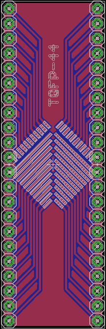
Eagle automatically cropped the image because there was nothing outside of that area.  Now, when I export the Gerber files, this is what I get:


image


The padding on the left and right appears in every Gerber viewer I've used, so it's definitely in the file, not just a rendering error on OSHPark's end.  After some messing around, I've confirmed that it's due to the QFP footprint and that it only occurs when it is rotated 45 degrees like that.  I made that footprint myself, and it is only SMD pads, no labels, no keepout, just the pads.  So why is the Gerber export so badly screwing up the board outline?  It only does it for the top layer, the bottom layer is the correct size.  Any thoughts?

  • Sign in to reply
  • Cancel
Parents
  • autodeskguest
    0 autodeskguest over 12 years ago

    Post your board file. I expect there is a library issue


    Warren

    --

    Web access to CadSoft support forums at www.eaglecentral.ca.  Where the CadSoft EAGLE community meets.


    • Cancel
    • Vote Up 0 Vote Down
    • Sign in to reply
    • Verify Answer
    • Cancel
Reply
  • autodeskguest
    0 autodeskguest over 12 years ago

    Post your board file. I expect there is a library issue


    Warren

    --

    Web access to CadSoft support forums at www.eaglecentral.ca.  Where the CadSoft EAGLE community meets.


    • Cancel
    • Vote Up 0 Vote Down
    • Sign in to reply
    • Verify Answer
    • Cancel
Children
No Data
element14 Community

element14 is the first online community specifically for engineers. Connect with your peers and get expert answers to your questions.

  • Members
  • Learn
  • Technologies
  • Challenges & Projects
  • Products
  • Store
  • About Us
  • Feedback & Support
  • FAQs
  • Terms of Use
  • Privacy Policy
  • Legal and Copyright Notices
  • Sitemap
  • Cookies

An Avnet Company © 2026 Premier Farnell Limited. All Rights Reserved.

Premier Farnell Ltd, registered in England and Wales (no 00876412), registered office: Farnell House, Forge Lane, Leeds LS12 2NE.

ICP 备案号 10220084.

Follow element14

  • X
  • Facebook
  • linkedin
  • YouTube