element14 Community
element14 Community
    Register Log In
  • Site
  • Search
  • Log In Register
  • Community Hub
    Community Hub
    • What's New on element14
    • Feedback and Support
    • Benefits of Membership
    • Personal Blogs
    • Members Area
    • Achievement Levels
  • Learn
    Learn
    • Ask an Expert
    • eBooks
    • element14 presents
    • Learning Center
    • Tech Spotlight
    • STEM Academy
    • Webinars, Training and Events
    • Learning Groups
  • Technologies
    Technologies
    • 3D Printing
    • FPGA
    • Industrial Automation
    • Internet of Things
    • Power & Energy
    • Sensors
    • Technology Groups
  • Challenges & Projects
    Challenges & Projects
    • Design Challenges
    • element14 presents Projects
    • Project14
    • Arduino Projects
    • Raspberry Pi Projects
    • Project Groups
  • Products
    Products
    • Arduino
    • Avnet Boards Community
    • Dev Tools
    • Manufacturers
    • Multicomp Pro
    • Product Groups
    • Raspberry Pi
    • RoadTests & Reviews
  • Store
    Store
    • Visit Your Store
    • Choose another store...
      • Europe
      •  Austria (German)
      •  Belgium (Dutch, French)
      •  Bulgaria (Bulgarian)
      •  Czech Republic (Czech)
      •  Denmark (Danish)
      •  Estonia (Estonian)
      •  Finland (Finnish)
      •  France (French)
      •  Germany (German)
      •  Hungary (Hungarian)
      •  Ireland
      •  Israel
      •  Italy (Italian)
      •  Latvia (Latvian)
      •  
      •  Lithuania (Lithuanian)
      •  Netherlands (Dutch)
      •  Norway (Norwegian)
      •  Poland (Polish)
      •  Portugal (Portuguese)
      •  Romania (Romanian)
      •  Russia (Russian)
      •  Slovakia (Slovak)
      •  Slovenia (Slovenian)
      •  Spain (Spanish)
      •  Sweden (Swedish)
      •  Switzerland(German, French)
      •  Turkey (Turkish)
      •  United Kingdom
      • Asia Pacific
      •  Australia
      •  China
      •  Hong Kong
      •  India
      •  Korea (Korean)
      •  Malaysia
      •  New Zealand
      •  Philippines
      •  Singapore
      •  Taiwan
      •  Thailand (Thai)
      • Americas
      •  Brazil (Portuguese)
      •  Canada
      •  Mexico (Spanish)
      •  United States
      Can't find the country/region you're looking for? Visit our export site or find a local distributor.
  • Translate
  • Profile
  • Settings
Autodesk EAGLE
  • Products
  • More
Autodesk EAGLE
EAGLE User Support (English) GND plane routing issues with custom SMD
  • Blog
  • Forum
  • Documents
  • Events
  • Polls
  • Files
  • Members
  • Mentions
  • Sub-Groups
  • Tags
  • More
  • Cancel
  • New
Join Autodesk EAGLE to participate - click to join for free!
Actions
  • Share
  • More
  • Cancel
Forum Thread Details
  • State Verified Answer
  • Replies 4 replies
  • Answers 1 answer
  • Subscribers 172 subscribers
  • Views 339 views
  • Users 0 members are here
  • ground_plane
  • custom_led
  • autoruter
  • surface-mount-led
Related

GND plane routing issues with custom SMD

Former Member
Former Member over 11 years ago

I've built a board with a number of custom SMD components on it (mostly little LED's), and am having an odd response from the routing of the GND/PWR planes that are run throughout for signal isolation. Everything is fine for the other SMD components (amps, gates etc), but the routing of the inner planes gets funky around the LED's. Is there something wrong with the custom components that could be causing this problem? They're pretty simple, and I built them with the same process that I used for the others.

image

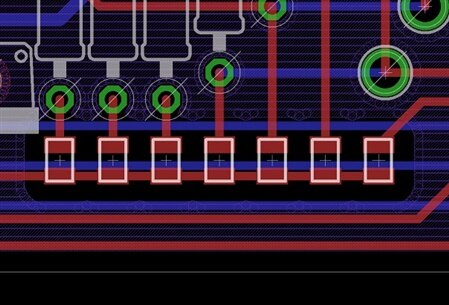
I should also note that the area is littered with DRC "Distance" errors, for both the Top and Bottom routing layers. This is also confusing to me, as the components should not interact with anything on the Bottom layer...


Thanks everyone


Edited to include DRC error information

  • Sign in to reply
  • Cancel
  • autodeskguest
    0 autodeskguest over 11 years ago

    Am 24.09.2013 23:48, schrieb Michael Stettenbenz:

    I've built a board with a number of custom SMD components on it (mostly

    little LED's), and am having an odd response from the routing of the

    GND/PWR planes that are run throughout for signal isolation. Everything

    is fine for the other smd componenets (amps, gates etc), but the routing

    of the inner planes gets funky around the LED's. Is there something

    wrong with the custom components that could be causing this problem?

    They're pretty simple, and I built them with the same process that I

    used for the others.


    Thanks everyone


    --

    To view any images and attachments in this post, visit:

    http://www.element14.com/community/message/89845#89845


    Is it possible that the outline of the LED is on layer 20 (dimension)?

    It seems to me that the color of the body from the resistors and the

    LEDs are not the same.


    Cheers Patrick


    • Cancel
    • Vote Up 0 Vote Down
    • Sign in to reply
    • Reject Answer
    • Cancel
  • dukepro
    0 dukepro over 11 years ago in reply to autodeskguest

    On 09/25/2013 02:10 AM, Patrick Steiner wrote:

    Am 24.09.2013 23:48, schrieb Michael Stettenbenz:

    I've built a board with a number of custom SMD components on it (mostly

    little LED's), and am having an odd response from the routing of the

    GND/PWR planes that are run throughout for signal isolation. Everything

    is fine for the other smd componenets (amps, gates etc), but the routing

    of the inner planes gets funky around the LED's. Is there something

    wrong with the custom components that could be causing this problem?

    They're pretty simple, and I built them with the same process that I

    used for the others.


    Thanks everyone


    --

    To view any images and attachments in this post, visit:

    http://www.element14.com/community/message/89845#89845


    Is it possible that the outline of the LED is on layer 20 (dimension)?

    It seems to me that the color of the body from the resistors and the

    LEDs are not the same.


    Cheers Patrick


    Instead of layer 20, you may have wanted to tPlace.


    I was looking at the pads of the resistors, as well.  It appears that

    they will short to the polygon on the inner layer.  Have you set the

    isolate value of the polygon?  It will probably get rid of some of the

    DRC errors.


        - Chuck


    • Cancel
    • Vote Up 0 Vote Down
    • Sign in to reply
    • Verify Answer
    • Reject Answer
    • Cancel
  • Former Member
    0 Former Member over 11 years ago in reply to autodeskguest

    Patrick, you got it in 1!

    Not quite sure how that happened, but I managed to lay down the dimensions using the wrong layer when I built the first LED, then duplicated the improperly built component for the different LED variations.

    I shifted all the dimension layers to the tPlace layer (as per Chuck), and the routing is now fixed thank you so much.


    Chuck,

    I hadn't done anything to modify the polygons after laying them down and you're correct, they auto'd to 0 isolation. I'm not dealing with too much power, but have bumped that isolation up to a value of .016. Thank you for that insight, I wouldn't have given it a second thought.


    Thanks again everyone, I really appreciate the quick and on point advice

    Mike

    • Cancel
    • Vote Up 0 Vote Down
    • Sign in to reply
    • Verify Answer
    • Cancel
  • dukepro
    0 dukepro over 11 years ago in reply to Former Member

    On 09/25/2013 02:24 PM, Michael Stettenbenz wrote:

    Chuck,

    I hadn't done anything to modify the polygons after laying them down and

    you're correct, they auto'd to 0 isolation.


    Michael,


    The polygons should have pulled back a certain distance anyway even with

    the isolation value at zero.  Setting that value on the polygon takes

    care of that particular polygon, but it does not address other

    clearances.  Double check your DRC->Clearance tab and make sure you have

    something reasonable there, as well.  The Wire-To-Pad distance may be

    sitting at zero, or close to it.


    Thanks again everyone, I really appreciate the quick and on point advice


    Glad to help out.


    Later,

        - Chuck


    • Cancel
    • Vote Up 0 Vote Down
    • Sign in to reply
    • Verify Answer
    • Cancel
element14 Community

element14 is the first online community specifically for engineers. Connect with your peers and get expert answers to your questions.

  • Members
  • Learn
  • Technologies
  • Challenges & Projects
  • Products
  • Store
  • About Us
  • Feedback & Support
  • FAQs
  • Terms of Use
  • Privacy Policy
  • Legal and Copyright Notices
  • Sitemap
  • Cookies

An Avnet Company © 2025 Premier Farnell Limited. All Rights Reserved.

Premier Farnell Ltd, registered in England and Wales (no 00876412), registered office: Farnell House, Forge Lane, Leeds LS12 2NE.

ICP 备案号 10220084.

Follow element14

  • X
  • Facebook
  • linkedin
  • YouTube