element14 Community
element14 Community
    Register Log In
  • Site
  • Search
  • Log In Register
  • Members
    Members
    • Achievement Levels
    • Benefits of Membership
    • Feedback and Support
    • Members Area
    • Personal Blogs
    • What's New on element14
  • Learn
    Learn
    • eBooks
    • Learning Center
    • Learning Groups
    • STEM Academy
    • Webinars, Training and Events
  • Technologies
    Technologies
    • 3D Printing
    • Experts & Guidance
    • FPGA
    • Industrial Automation
    • Internet of Things
    • Power & Energy
    • Sensors
    • Technology Groups
  • Challenges & Projects
    Challenges & Projects
    • Arduino Projects
    • Design Challenges
    • element14 presents
    • Project14
    • Project Groups
    • Raspberry Pi Projects
  • Products
    Products
    • Arduino
    • Avnet Boards Community
    • Dev Tools
    • Manufacturers
    • Product Groups
    • Raspberry Pi
    • RoadTests & Reviews
  • Store
    Store
    • Visit Your Store
    • Or choose another store...
      • Europe
      •  Austria (German)
      •  Belgium (Dutch, French)
      •  Bulgaria (Bulgarian)
      •  Czech Republic (Czech)
      •  Denmark (Danish)
      •  Estonia (Estonian)
      •  Finland (Finnish)
      •  France (French)
      •  Germany (German)
      •  Hungary (Hungarian)
      •  Ireland
      •  Israel
      •  Italy (Italian)
      •  Latvia (Latvian)
      •  
      •  Lithuania (Lithuanian)
      •  Netherlands (Dutch)
      •  Norway (Norwegian)
      •  Poland (Polish)
      •  Portugal (Portuguese)
      •  Romania (Romanian)
      •  Russia (Russian)
      •  Slovakia (Slovak)
      •  Slovenia (Slovenian)
      •  Spain (Spanish)
      •  Sweden (Swedish)
      •  Switzerland(German, French)
      •  Turkey (Turkish)
      •  United Kingdom
      • Asia Pacific
      •  Australia
      •  China
      •  Hong Kong
      •  India
      •  Korea (Korean)
      •  Malaysia
      •  New Zealand
      •  Philippines
      •  Singapore
      •  Taiwan
      •  Thailand (Thai)
      • Americas
      •  Brazil (Portuguese)
      •  Canada
      •  Mexico (Spanish)
      •  United States
      Can't find the country/region you're looking for? Visit our export site or find a local distributor.
  • Translate
  • Profile
Autodesk EAGLE
  • Products
  • More
Autodesk EAGLE
EAGLE User Support (English) Molex KK connectors: wrong pitch?
  • Blog
  • Forum
  • Documents
  • Events
  • Polls
  • Files
  • Members
  • Mentions
  • Sub-Groups
  • Tags
  • More
  • Cancel
  • New
Autodesk EAGLE requires membership for participation - click to join
Actions
  • Share
  • More
  • Cancel
Forum Thread Details
  • State Not Answered
  • Replies 9 replies
  • Subscribers 146 subscribers
  • Views 547 views
  • Users 0 members are here
Related

Molex KK connectors: wrong pitch?

Former Member
Former Member over 9 years ago

Hi,

I´m trying to use the Molex KK-156 headers from the con-molex lib on my board. From their title I expected them to have the 1,56" pitch,

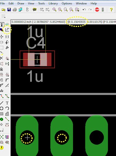
but if I use the measuring feature in EAGLE it always tells me that the pitch is 1".

Am I doing something wrong, is it an error in the lib (my con-molex.lib is dated 12/13/2011)?


Hope somebody can help me.....


Herbert

  • Sign in to reply
  • Cancel
  • element14jamie
    0 element14jamie over 9 years ago

    Hello Herbert,

    Welcome to the element14 Community, we hope you are enjoying it so far!! I will move this question over to the CadSoft EAGLE Support area as it is a better fit.


    Thank you,


    Jamie

    • Cancel
    • Vote Up 0 Vote Down
    • Sign in to reply
    • Verify Answer
    • Cancel
  • Former Member
    0 Former Member over 9 years ago in reply to element14jamie

    Thanks Jamie


    Of course in my question I was referring to .156" and .1". Sorry for the typos.

    • Cancel
    • Vote Up 0 Vote Down
    • Sign in to reply
    • Verify Answer
    • Cancel
  • shabaz
    0 shabaz over 9 years ago in reply to Former Member

    Hi Herbert,


    I see of the order of 0.156" (I used KK-156-14 component as an example). You likely have the grid set to 0.1" and your measurements are of that granularity. Reducing the grid will give you the granularity you want.

    By the way, you could measure it exactly by inspecting the library and clicking on 'info' for each pad that makes up the component (this will reveal

    the X and Y co-ords for the pad).

    • Cancel
    • Vote Up 0 Vote Down
    • Sign in to reply
    • Verify Answer
    • Cancel
  • Former Member
    0 Former Member over 9 years ago in reply to shabaz

    I reduced the grid to 0.01 inch but for some reason the measurement for this part still shows 2.54 mm between to pins??  I´m confused......image


    image   image

    • Cancel
    • Vote Up 0 Vote Down
    • Sign in to reply
    • Verify Answer
    • Cancel
  • shabaz
    0 shabaz over 9 years ago in reply to Former Member

    This is what I see when the ref is set close to a pin, and then I measure to the adjacent pin.

    I used part KK-156-14 from con-molex.

    image

    • Cancel
    • Vote Up 0 Vote Down
    • Sign in to reply
    • Verify Answer
    • Cancel
  • Former Member
    0 Former Member over 9 years ago in reply to shabaz

    hmm, I´m doing the measurements in the circuit view, not in the board view - is that the wrong approach? Sorry for those newbie questions.....  image

    • Cancel
    • Vote Up 0 Vote Down
    • Sign in to reply
    • Verify Answer
    • Cancel
  • shabaz
    0 shabaz over 9 years ago

    Hi Herbert,


    That's correct, it is only done in the board view (i.e. physical view). For the schematic view (i.e. logical view), the grid setting should never be changed (it affects net connectivity when you place nets) so you will need to change back to the default setting of 0.1 in the schematic view.

    • Cancel
    • Vote Up 0 Vote Down
    • Sign in to reply
    • Verify Answer
    • Cancel
  • autodeskguest
    0 autodeskguest over 9 years ago in reply to Former Member

    On 25/03/14 22:51, Herbert Koller wrote:

    hmm, I´m doing the measurements in the circuit view, not in the board

    view - is that the wrong approach?


    Yes.


    The "circuit view" is more properly called the "schematic editor"


    From OED:

        schematic

        (Of a diagram or other representation) symbolic and simplified


    This editor deals with the schematic design, which is a symbolic

    representation of the circuit's function, and has no connection to the

    physical shape or dimension. Indeed for many components the "symbol" on

    the schematic might map to one of a dozen or more "packages" you can

    choose between.


    So when you consider that, it's fairly clear that you can't measure the

    gap between physical package pins on the schematic!


    • Cancel
    • Vote Up 0 Vote Down
    • Sign in to reply
    • Verify Answer
    • Cancel
  • Former Member
    0 Former Member over 9 years ago in reply to autodeskguest

    Hello folks,

    thank you very much for all your help in getting better with EAGLE.

    You helped me a lot. And soory again for those newbie questions.

    Herbert

    • Cancel
    • Vote Up 0 Vote Down
    • Sign in to reply
    • Verify Answer
    • Cancel
element14 Community

element14 is the first online community specifically for engineers. Connect with your peers and get expert answers to your questions.

  • Members
  • Learn
  • Technologies
  • Challenges & Projects
  • Products
  • Store
  • About Us
  • Feedback & Support
  • FAQs
  • Terms of Use
  • Privacy Policy
  • Legal and Copyright Notices
  • Sitemap
  • Cookies

An Avnet Company © 2023 Premier Farnell Limited. All Rights Reserved.

Premier Farnell Ltd, registered in England and Wales (no 00876412), registered office: Farnell House, Forge Lane, Leeds LS12 2NE.

ICP 备案号 10220084.

Follow element14

  • X
  • Facebook
  • linkedin
  • YouTube