element14 Community
element14 Community
    Register Log In
  • Site
  • Search
  • Log In Register
  • Community Hub
    Community Hub
    • What's New on element14
    • Feedback and Support
    • Benefits of Membership
    • Personal Blogs
    • Members Area
    • Achievement Levels
  • Learn
    Learn
    • Ask an Expert
    • eBooks
    • element14 presents
    • Learning Center
    • Tech Spotlight
    • STEM Academy
    • Webinars, Training and Events
    • Learning Groups
  • Technologies
    Technologies
    • 3D Printing
    • FPGA
    • Industrial Automation
    • Internet of Things
    • Power & Energy
    • Sensors
    • Technology Groups
  • Challenges & Projects
    Challenges & Projects
    • Design Challenges
    • element14 presents Projects
    • Project14
    • Arduino Projects
    • Raspberry Pi Projects
    • Project Groups
  • Products
    Products
    • Arduino
    • Avnet & Tria Boards Community
    • Dev Tools
    • Manufacturers
    • Multicomp Pro
    • Product Groups
    • Raspberry Pi
    • RoadTests & Reviews
  • About Us
  • Store
    Store
    • Visit Your Store
    • Choose another store...
      • Europe
      •  Austria (German)
      •  Belgium (Dutch, French)
      •  Bulgaria (Bulgarian)
      •  Czech Republic (Czech)
      •  Denmark (Danish)
      •  Estonia (Estonian)
      •  Finland (Finnish)
      •  France (French)
      •  Germany (German)
      •  Hungary (Hungarian)
      •  Ireland
      •  Israel
      •  Italy (Italian)
      •  Latvia (Latvian)
      •  
      •  Lithuania (Lithuanian)
      •  Netherlands (Dutch)
      •  Norway (Norwegian)
      •  Poland (Polish)
      •  Portugal (Portuguese)
      •  Romania (Romanian)
      •  Russia (Russian)
      •  Slovakia (Slovak)
      •  Slovenia (Slovenian)
      •  Spain (Spanish)
      •  Sweden (Swedish)
      •  Switzerland(German, French)
      •  Turkey (Turkish)
      •  United Kingdom
      • Asia Pacific
      •  Australia
      •  China
      •  Hong Kong
      •  India
      • Japan
      •  Korea (Korean)
      •  Malaysia
      •  New Zealand
      •  Philippines
      •  Singapore
      •  Taiwan
      •  Thailand (Thai)
      • Vietnam
      • Americas
      •  Brazil (Portuguese)
      •  Canada
      •  Mexico (Spanish)
      •  United States
      Can't find the country/region you're looking for? Visit our export site or find a local distributor.
  • Translate
  • Profile
  • Settings
Autodesk EAGLE
  • Products
  • More
Autodesk EAGLE
EAGLE User Support (English) Questions regarding 2+ layer PCB design
  • Blog
  • Forum
  • Documents
  • Events
  • Polls
  • Files
  • Members
  • Mentions
  • Sub-Groups
  • Tags
  • More
  • Cancel
  • New
Join Autodesk EAGLE to participate - click to join for free!
Actions
  • Share
  • More
  • Cancel
Forum Thread Details
  • State Not Answered
  • Replies 3 replies
  • Subscribers 179 subscribers
  • Views 483 views
  • Users 0 members are here
  • eagle
  • pcb
  • via
  • layers
Related

Questions regarding 2+ layer PCB design

Former Member
Former Member over 11 years ago

Hello, I've done 4 layer projects successfully using EPCB and their software.


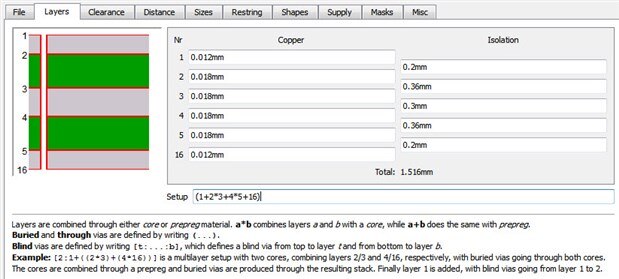
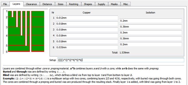
Now I'm converting the project to 6 layers, with added capabilities, and have chosen Eagle since the board manufacturer I've had to switch to favors this program. I've downloaded the manufacturer's .dru file for a  6 layer board. Now I'm trying to figure out how to assign which layer a via connects to. Presently, the .dru file is only letting me connect from the top to the bottom layers.


Also, since this project uses 256-pin BGA's I don't use schematics. I would like to do this starting from scratch in PCB design.


So how do I go about assign a layer to a via? Thanks

  • Sign in to reply
  • Cancel
Parents
  • kikoun
    0 kikoun over 11 years ago

    Hi,

    You have to edit the DRU file (DRC, 'layers' tab). You have to configure the stacking, in away that you could have buried and/or blind via. But check with your manufacturer, that he will be able to build your PCB (unless you really like bad surprises !)

    Guillaume.

    • Cancel
    • Vote Up 0 Vote Down
    • Sign in to reply
    • Verify Answer
    • Cancel
  • Former Member
    0 Former Member over 11 years ago in reply to kikoun

    Hi Guillaume,

         Thanks for your response. I will contact them soon as a prospective board manufacturer, but since I'm a hobbyist I don't want to look "ignorant", so I try to gather more information in this new endeavor. This is the result of loading their .dru file:


    image

    Should it look more like this? There are no buried vias in this design, just straight drilling through all layers for all vias, just that the vias may connect to one or more layers from the top to any layer below....

    image

    • Cancel
    • Vote Up 0 Vote Down
    • Sign in to reply
    • Verify Answer
    • Cancel
  • kikoun
    0 kikoun over 11 years ago in reply to Former Member

    HI,

    In your second design you don't have buried via, just normal via and blind via.

    The normal via is standard and really common. But blind via is less common, and you have to be sure that your manufacturer can do it, and if you don't have additional charges for blind via.

    Usually the stacking is symmetrical, if it's possible, through holes are plated after pressing all layer, except for buried via (need a to be plated before pressing external layer -> extra cost).

    But for blind via I don't know if there is extra cost. Let me know !

    Guillaume.

    • Cancel
    • Vote Up 0 Vote Down
    • Sign in to reply
    • Verify Answer
    • Cancel
Reply
  • kikoun
    0 kikoun over 11 years ago in reply to Former Member

    HI,

    In your second design you don't have buried via, just normal via and blind via.

    The normal via is standard and really common. But blind via is less common, and you have to be sure that your manufacturer can do it, and if you don't have additional charges for blind via.

    Usually the stacking is symmetrical, if it's possible, through holes are plated after pressing all layer, except for buried via (need a to be plated before pressing external layer -> extra cost).

    But for blind via I don't know if there is extra cost. Let me know !

    Guillaume.

    • Cancel
    • Vote Up 0 Vote Down
    • Sign in to reply
    • Verify Answer
    • Cancel
Children
No Data
element14 Community

element14 is the first online community specifically for engineers. Connect with your peers and get expert answers to your questions.

  • Members
  • Learn
  • Technologies
  • Challenges & Projects
  • Products
  • Store
  • About Us
  • Feedback & Support
  • FAQs
  • Terms of Use
  • Privacy Policy
  • Legal and Copyright Notices
  • Sitemap
  • Cookies

An Avnet Company © 2025 Premier Farnell Limited. All Rights Reserved.

Premier Farnell Ltd, registered in England and Wales (no 00876412), registered office: Farnell House, Forge Lane, Leeds LS12 2NE.

ICP 备案号 10220084.

Follow element14

  • X
  • Facebook
  • linkedin
  • YouTube