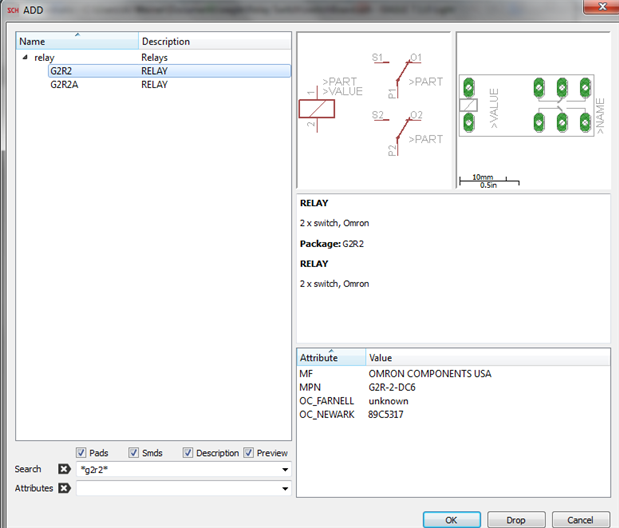
I am trying to design a small board (my first) that incorporates three G2R2 relays. I found the component in the "add" section but it appears that the schematic and the board drawings are different, specifically the N.O. and N.C. contacts. The actual part has the N.C. contact as the one closest to the coil (as shown in the board image). I am miss-reading the two images or is it as simple as rotating the N.O-Com-N.C. connection in the schematic? Or is there something else? It seems odd that the two images wouldn't have the components lined up. I attached a screenshot of the G2R2 part images. Thanks.