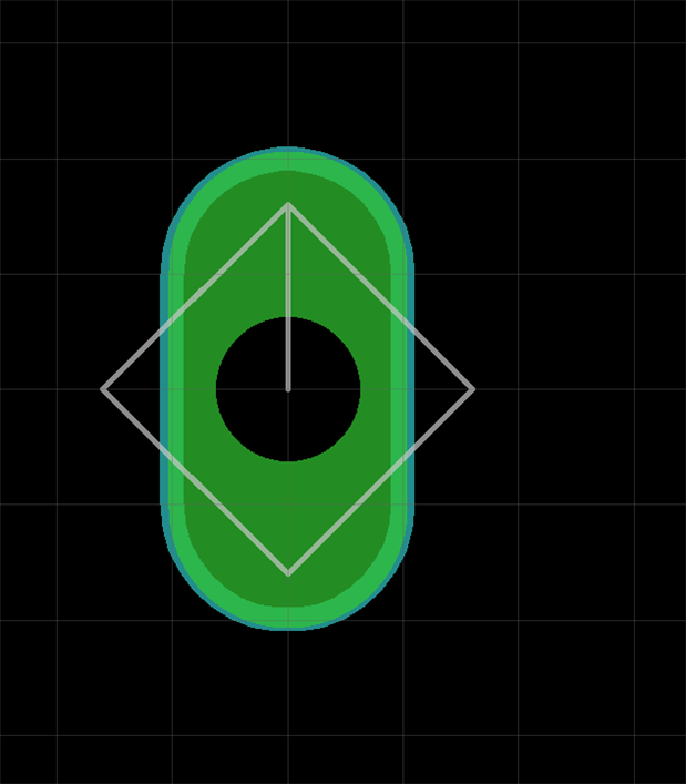
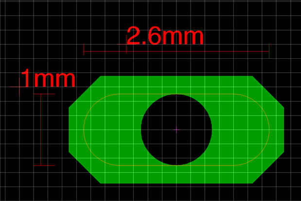
I am making a usb type A-B library device. Attachment is the link to the datasheet. I need to make 2 oval holes but I cannot figure out how to do it. I can only use the round and square pad. Do you have any suggestion of how to do this? Thank you so much.
Attachments:
| Molex Micro USB A-B SMT 0475900001.pdf |