element14 Community
element14 Community
    Register Log In
  • Site
  • Search
  • Log In Register
  • Community Hub
    Community Hub
    • What's New on element14
    • Feedback and Support
    • Benefits of Membership
    • Personal Blogs
    • Members Area
    • Achievement Levels
  • Learn
    Learn
    • Ask an Expert
    • eBooks
    • element14 presents
    • Learning Center
    • Tech Spotlight
    • STEM Academy
    • Webinars, Training and Events
    • Learning Groups
  • Technologies
    Technologies
    • 3D Printing
    • FPGA
    • Industrial Automation
    • Internet of Things
    • Power & Energy
    • Sensors
    • Technology Groups
  • Challenges & Projects
    Challenges & Projects
    • Design Challenges
    • element14 presents Projects
    • Project14
    • Arduino Projects
    • Raspberry Pi Projects
    • Project Groups
  • Products
    Products
    • Arduino
    • Avnet Boards Community
    • Dev Tools
    • Manufacturers
    • Multicomp Pro
    • Product Groups
    • Raspberry Pi
    • RoadTests & Reviews
  • Store
    Store
    • Visit Your Store
    • Choose another store...
      • Europe
      •  Austria (German)
      •  Belgium (Dutch, French)
      •  Bulgaria (Bulgarian)
      •  Czech Republic (Czech)
      •  Denmark (Danish)
      •  Estonia (Estonian)
      •  Finland (Finnish)
      •  France (French)
      •  Germany (German)
      •  Hungary (Hungarian)
      •  Ireland
      •  Israel
      •  Italy (Italian)
      •  Latvia (Latvian)
      •  
      •  Lithuania (Lithuanian)
      •  Netherlands (Dutch)
      •  Norway (Norwegian)
      •  Poland (Polish)
      •  Portugal (Portuguese)
      •  Romania (Romanian)
      •  Russia (Russian)
      •  Slovakia (Slovak)
      •  Slovenia (Slovenian)
      •  Spain (Spanish)
      •  Sweden (Swedish)
      •  Switzerland(German, French)
      •  Turkey (Turkish)
      •  United Kingdom
      • Asia Pacific
      •  Australia
      •  China
      •  Hong Kong
      •  India
      •  Korea (Korean)
      •  Malaysia
      •  New Zealand
      •  Philippines
      •  Singapore
      •  Taiwan
      •  Thailand (Thai)
      • Americas
      •  Brazil (Portuguese)
      •  Canada
      •  Mexico (Spanish)
      •  United States
      Can't find the country/region you're looking for? Visit our export site or find a local distributor.
  • Translate
  • Profile
  • Settings
Autodesk EAGLE
  • Products
  • More
Autodesk EAGLE
EAGLE User Support (English) Trying to create solid odd shaped pads
  • Blog
  • Forum
  • Documents
  • Events
  • Polls
  • Files
  • Members
  • Mentions
  • Sub-Groups
  • Tags
  • More
  • Cancel
  • New
Join Autodesk EAGLE to participate - click to join for free!
Actions
  • Share
  • More
  • Cancel
Forum Thread Details
  • State Not Answered
  • Replies 2 replies
  • Subscribers 171 subscribers
  • Views 388 views
  • Users 0 members are here
Related

Trying to create solid odd shaped pads

talon2000
talon2000 over 10 years ago

First time using Eagle, so I'm not all that familiar with it yet. It seems to be more of a PITA than anything.


I've got the pads drawn and in a dxf format. Which I used for my prototype milling machine, but now I'm wanting to actually have boards made for production.


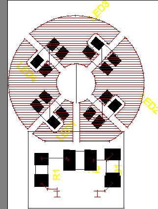
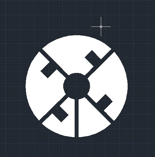
I am able to draw out the standard pad layout which is in a circle but I'm not able to create larger pads for some of them to fill the circle. I attached the brd file showing the basic layout of the smd pads. 4 pads per device at an angle on the circle divided into sections see the .dxf file.

Here's a rough drawing. The part in green is where I want to make the current SMD pads extend to. Sorry the drawing was done in MS paint since I can't seem to get this done in EC. The parts will make the connections, and the larger SMD pad will be for heat dissipation. The second picture is what the actual pads look like. I would like to keep the original Solder mask of the original smd pads, so the new pads get mostly covered.


I hope this makes sense, like I sad this is my first project, and first time  using eagle cad.


imageimage


Forums wouldn't let me post the DXF file.

Attachments:
splpad.zip
  • Sign in to reply
  • Cancel
  • Former Member
    0 Former Member over 10 years ago
    I have I make pcb in the eagle roughly 9 month
    From then that I changed the eagle with a new cad
    I tryed with your own pcb see the result
    Dxf export from the eagle it is very off-hand and bad quality


    imageimage


    Attachments:
    SPL-1-test.rar
    • Cancel
    • Vote Up 0 Vote Down
    • Sign in to reply
    • Verify Answer
    • Cancel
  • autodeskguest
    0 autodeskguest over 10 years ago

    Hi Kevin,


    I hope you're doing well. Whenever possible try to use one of the

    default pad shapes (SMD, Square, Round, Octagon, Long, or Offset).

    Whenever you need any oddly shaped pad, you can use one of the standard

    shapes and then extend it with a polygon in the library. This is the

    Arbitrary pad shapes features. Section 8.13 of the eagle manual covers

    doing this in detail.


    DXF import is 90% of the time used to bring in complex board geometries

    so that a PCB can be made to suite an enclosure.


    Let me know if there's anything else I can do for you.


    Best Regards,

    Jorge Garcia


    • Cancel
    • Vote Up 0 Vote Down
    • Sign in to reply
    • Verify Answer
    • Cancel
element14 Community

element14 is the first online community specifically for engineers. Connect with your peers and get expert answers to your questions.

  • Members
  • Learn
  • Technologies
  • Challenges & Projects
  • Products
  • Store
  • About Us
  • Feedback & Support
  • FAQs
  • Terms of Use
  • Privacy Policy
  • Legal and Copyright Notices
  • Sitemap
  • Cookies

An Avnet Company © 2025 Premier Farnell Limited. All Rights Reserved.

Premier Farnell Ltd, registered in England and Wales (no 00876412), registered office: Farnell House, Forge Lane, Leeds LS12 2NE.

ICP 备案号 10220084.

Follow element14

  • X
  • Facebook
  • linkedin
  • YouTube