element14 Community
element14 Community
    Register Log In
  • Site
  • Search
  • Log In Register
  • Community Hub
    Community Hub
    • What's New on element14
    • Feedback and Support
    • Benefits of Membership
    • Personal Blogs
    • Members Area
    • Achievement Levels
  • Learn
    Learn
    • Ask an Expert
    • eBooks
    • element14 presents
    • Learning Center
    • Tech Spotlight
    • STEM Academy
    • Webinars, Training and Events
    • Learning Groups
  • Technologies
    Technologies
    • 3D Printing
    • FPGA
    • Industrial Automation
    • Internet of Things
    • Power & Energy
    • Sensors
    • Technology Groups
  • Challenges & Projects
    Challenges & Projects
    • Design Challenges
    • element14 presents Projects
    • Project14
    • Arduino Projects
    • Raspberry Pi Projects
    • Project Groups
  • Products
    Products
    • Arduino
    • Avnet & Tria Boards Community
    • Dev Tools
    • Manufacturers
    • Multicomp Pro
    • Product Groups
    • Raspberry Pi
    • RoadTests & Reviews
  • About Us
  • Store
    Store
    • Visit Your Store
    • Choose another store...
      • Europe
      •  Austria (German)
      •  Belgium (Dutch, French)
      •  Bulgaria (Bulgarian)
      •  Czech Republic (Czech)
      •  Denmark (Danish)
      •  Estonia (Estonian)
      •  Finland (Finnish)
      •  France (French)
      •  Germany (German)
      •  Hungary (Hungarian)
      •  Ireland
      •  Israel
      •  Italy (Italian)
      •  Latvia (Latvian)
      •  
      •  Lithuania (Lithuanian)
      •  Netherlands (Dutch)
      •  Norway (Norwegian)
      •  Poland (Polish)
      •  Portugal (Portuguese)
      •  Romania (Romanian)
      •  Russia (Russian)
      •  Slovakia (Slovak)
      •  Slovenia (Slovenian)
      •  Spain (Spanish)
      •  Sweden (Swedish)
      •  Switzerland(German, French)
      •  Turkey (Turkish)
      •  United Kingdom
      • Asia Pacific
      •  Australia
      •  China
      •  Hong Kong
      •  India
      •  Korea (Korean)
      •  Malaysia
      •  New Zealand
      •  Philippines
      •  Singapore
      •  Taiwan
      •  Thailand (Thai)
      • Americas
      •  Brazil (Portuguese)
      •  Canada
      •  Mexico (Spanish)
      •  United States
      Can't find the country/region you're looking for? Visit our export site or find a local distributor.
  • Translate
  • Profile
  • Settings
Autodesk EAGLE
  • Products
  • More
Autodesk EAGLE
Forum Atmega328 - Newbie design
  • Blog
  • Forum
  • Documents
  • Events
  • Polls
  • Files
  • Members
  • Mentions
  • Sub-Groups
  • Tags
  • More
  • Cancel
  • New
Join Autodesk EAGLE to participate - click to join for free!
Actions
  • Share
  • More
  • Cancel
Forum Thread Details
  • State Verified Answer
  • Replies 14 replies
  • Answers 1 answer
  • Subscribers 179 subscribers
  • Views 1365 views
  • Users 0 members are here
Related

Atmega328 - Newbie design

anishkgt
anishkgt over 9 years ago

Hi All,


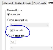
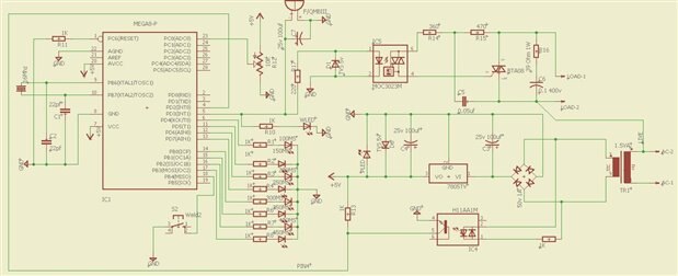
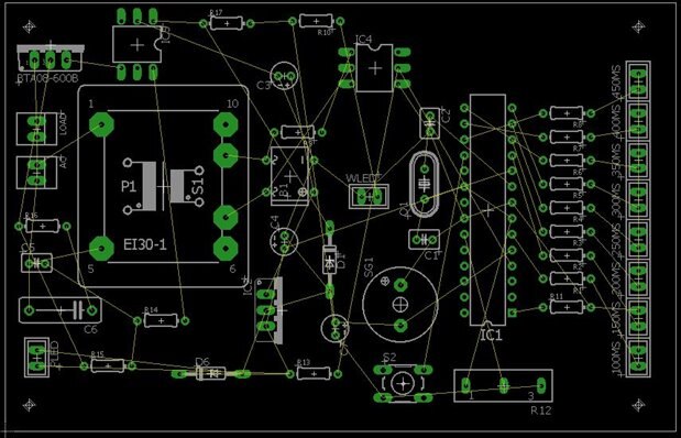
A little new to the Eagle PCB, so please bear with my silly questions. I had designed a single sided board and all ready for etching. Printed the circuit on paper, only to find out that ATmega328 does not fit in the printout. Download all available libraries of eagle and non seem to be working.


Any help would be appreciated.

  • Sign in to reply
  • Cancel

Top Replies

  • jc2048
    jc2048 over 9 years ago in reply to anishkgt +2 suggested
    That's a horrible layout (in my opinion). Did an autorouter do it? If the primary of your transformer has mains on it, you need much better spacing there than the minimum default setting. The ground layout…
  • michaelkellett
    0 michaelkellett over 9 years ago

    Are you sure that your printer is printing at exactly 1:1 ratio - check the board overall dimensions to scale the printer.


    MK

    • Cancel
    • Vote Up 0 Vote Down
    • Sign in to reply
    • Verify Answer
    • Cancel
  • anishkgt
    0 anishkgt over 9 years ago in reply to michaelkellett

    All were working earlier. now all of a sudden its happening. I've also re-installed eagle. Below is the dimensions in mmimage

    image

    • Cancel
    • Vote Up 0 Vote Down
    • Sign in to reply
    • Verify Answer
    • Cancel
  • michaelkellett
    0 michaelkellett over 9 years ago in reply to anishkgt

    So when you print it what does the 109.22 dimension actually measure with a ruler ?


    MK

    • Cancel
    • Vote Up 0 Vote Down
    • Sign in to reply
    • Verify Answer
    • Cancel
  • jc2048
    0 jc2048 over 9 years ago in reply to anishkgt

    That's a horrible layout (in my opinion). Did an autorouter do it? If the primary of your transformer has mains on it, you need much better spacing there than the minimum default setting. The ground layout on the secondary side could be much better too. Having the output cap for the regulator up next to the switches at the top seems like an odd placement. You might also want to increase the widths of the tracks (for current handling ability) around the load switch and the snubber components. The isolation figure for the opto device controlling the triac is meaningless if you push tracks from the low voltage side between the pins on the high voltage side.


    If you have to have a single-sided layout, perhaps consider a few wire links on the top rather than the very convoluted paths on the bottom layer.


    Sorry if that sounds like a bit of a brutal critique. It's meant to be helpful (so you can improve the layout) rather than stop you in your tracks (so to speak).

    • Cancel
    • Vote Up +2 Vote Down
    • Sign in to reply
    • Verify Answer
    • Reject Answer
    • Cancel
  • shabaz
    0 shabaz over 9 years ago in reply to jc2048

    Hi Jon!


    Yes, that's a typical output from its auto-router. You soon recognise the 'style' of its output : )

    • Cancel
    • Vote Up 0 Vote Down
    • Sign in to reply
    • Verify Answer
    • Cancel
  • anishkgt
    0 anishkgt over 9 years ago in reply to michaelkellett

    Thanks guys for the feedback. Am just getting starting, taking those baby steps.


    Figured the printout size, it was the generic driver that the printer had. Changed it to the recommended driver and all works well. Was gonna etch it today. Will hold it back.

    • Cancel
    • Vote Up 0 Vote Down
    • Sign in to reply
    • Verify Answer
    • Cancel
  • michaelkellett
    0 michaelkellett over 9 years ago in reply to jc2048

    You're absolutely right - I was just responding to the dimension issue and I didn't look at the circuit itself.


    @George, Google "ipc mains clearances" - you'll get lots of hits which will give some idea as to what a board with mains on it should look like.  Before you do put mains on your own pcb do please post it here again - for more good, if tough, advice.


    MK

    • Cancel
    • Vote Up 0 Vote Down
    • Sign in to reply
    • Verify Answer
    • Cancel
  • anishkgt
    0 anishkgt over 9 years ago in reply to jc2048

    Hi Jon,


    Would you be having a documentation or provide me some tips to place the components. I have downloaded the autoplace_v3.ulp to see it can help but that returned an error "access open c:\windows\system32\place.scr". Any idea how i can resolve this.

    • Cancel
    • Vote Up 0 Vote Down
    • Sign in to reply
    • Verify Answer
    • Cancel
  • anishkgt
    0 anishkgt over 9 years ago in reply to anishkgt

    So far I've got this from what I could gather reading. Maybe not best placement but would this be ok.image

    • Cancel
    • Vote Up 0 Vote Down
    • Sign in to reply
    • Verify Answer
    • Cancel
  • jc2048
    0 jc2048 over 9 years ago in reply to anishkgt

    [I wrote this quickly before seeing your subsequent post, so this refers to your first layout.]


    Sorry, I realise I didn't phrase that very well. I was referring to the track layout - the component placement isn't all that bad. Parts are mostly where they need to be with some exceptions. Remember I can't see your circuit and I'm reconstructing it in my head from the layout.


    The capacitor on the output of the bridge rectifier needs to be right there at the output. Perhaps make it a 5mm pitch part (or bend the legs of a 2.5mm part to fit a 5mm placement).


    It looks like the crystal and its load capacitors are on the wrong side of the processor. The tracks to the crystal should be short.


    It doesn't look like there's a decoupling cap for the processor - certainly not one in the right place (next to the supply pin)


    What are the resistors with the links doing? They don't seem to be pull-ups. Are they necessary?


    Imagine a line 5mm wide drawn vertically up through the centre of the opto driver for the triac the full height of th eboard. Try and get all the mains stuff on one side and all the low voltage stuff on the other and nothing on the line. Think of it as a moat that nothing can cross except the transformer and opto driver acting as bridges. That gives you a reasonable minimum level of primary to secondary isolation on the board.


    Move the PLED connector across so that it's not with the mains stuff.


    I'd use a wider pin pitch than 2.54mm for the AC and LOAD connectors. 3.95(?) or 5.12 would be better.


    On the mains side go for as much clearance as possible. You certainly don't want the situation where the tracks wind round the connectors with 0.15mm or 0.2mm spacing. The situation with the triac, where the track from the top pin slopes down and comes to within the minimum spacing of the centre, is out too.


    To get a sensible track layout for something like this you need to do it by hand.


    What is the fuse rating of the load circuit? That tells us the maximum continuous current and we can then tell you the minimum track width you'll need to carry it.

    • Cancel
    • Vote Up 0 Vote Down
    • Sign in to reply
    • Verify Answer
    • Cancel
>
element14 Community

element14 is the first online community specifically for engineers. Connect with your peers and get expert answers to your questions.

  • Members
  • Learn
  • Technologies
  • Challenges & Projects
  • Products
  • Store
  • About Us
  • Feedback & Support
  • FAQs
  • Terms of Use
  • Privacy Policy
  • Legal and Copyright Notices
  • Sitemap
  • Cookies

An Avnet Company © 2025 Premier Farnell Limited. All Rights Reserved.

Premier Farnell Ltd, registered in England and Wales (no 00876412), registered office: Farnell House, Forge Lane, Leeds LS12 2NE.

ICP 备案号 10220084.

Follow element14

  • X
  • Facebook
  • linkedin
  • YouTube