Finally motivated myself into trying Eagle files only to see my original instincts told me NOT to bother.
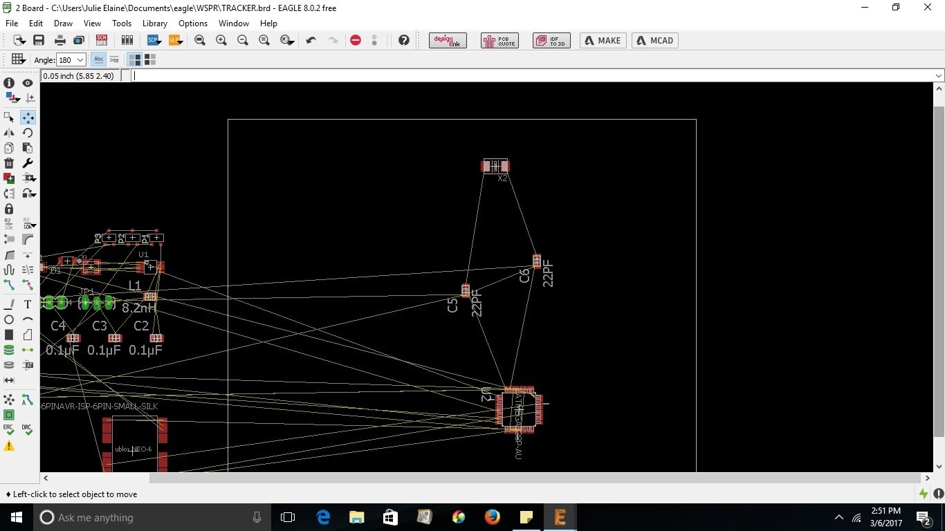
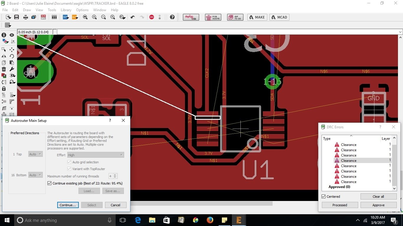
The last thing I expected was not finding common components in the library.My first mistake to assume that an Atmega328p-au would be one of the easiest to find.Not so and had to search the ends of the earth to find it and manually place it into the LIBR directory.After a 4 hour search and finally having this IC in my schematic layout I now see"shorts on several pins of this chip in the BRD window.The worse possible places no less on 3.3v and ground
I can probably modify this file but now getting far deeper into a simple project I thought would be straight forward.
Is it a software glitch causing this or a bad library file ?
Anyone know where to find a working Atmega328p-au footprint
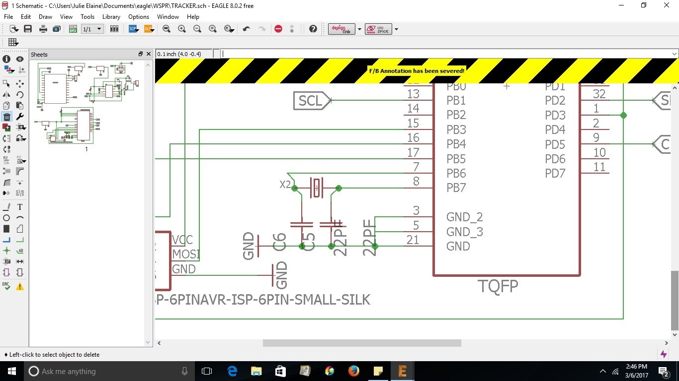
See attached screen shot of the issue.