element14 Community
element14 Community
    Register Log In
  • Site
  • Search
  • Log In Register
  • Community Hub
    Community Hub
    • What's New on element14
    • Feedback and Support
    • Benefits of Membership
    • Personal Blogs
    • Members Area
    • Achievement Levels
  • Learn
    Learn
    • Ask an Expert
    • eBooks
    • element14 presents
    • Learning Center
    • Tech Spotlight
    • STEM Academy
    • Webinars, Training and Events
    • Learning Groups
  • Technologies
    Technologies
    • 3D Printing
    • FPGA
    • Industrial Automation
    • Internet of Things
    • Power & Energy
    • Sensors
    • Technology Groups
  • Challenges & Projects
    Challenges & Projects
    • Design Challenges
    • element14 presents Projects
    • Project14
    • Arduino Projects
    • Raspberry Pi Projects
    • Project Groups
  • Products
    Products
    • Arduino
    • Avnet & Tria Boards Community
    • Dev Tools
    • Manufacturers
    • Multicomp Pro
    • Product Groups
    • Raspberry Pi
    • RoadTests & Reviews
  • About Us
    About the element14 Community
  • Store
    Store
    • Visit Your Store
    • Choose another store...
      • Europe
      •  Austria (German)
      •  Belgium (Dutch, French)
      •  Bulgaria (Bulgarian)
      •  Czech Republic (Czech)
      •  Denmark (Danish)
      •  Estonia (Estonian)
      •  Finland (Finnish)
      •  France (French)
      •  Germany (German)
      •  Hungary (Hungarian)
      •  Ireland
      •  Israel
      •  Italy (Italian)
      •  Latvia (Latvian)
      •  
      •  Lithuania (Lithuanian)
      •  Netherlands (Dutch)
      •  Norway (Norwegian)
      •  Poland (Polish)
      •  Portugal (Portuguese)
      •  Romania (Romanian)
      •  Russia (Russian)
      •  Slovakia (Slovak)
      •  Slovenia (Slovenian)
      •  Spain (Spanish)
      •  Sweden (Swedish)
      •  Switzerland(German, French)
      •  Turkey (Turkish)
      •  United Kingdom
      • Asia Pacific
      •  Australia
      •  China
      •  Hong Kong
      •  India
      •  Japan
      •  Korea (Korean)
      •  Malaysia
      •  New Zealand
      •  Philippines
      •  Singapore
      •  Taiwan
      •  Thailand (Thai)
      •  Vietnam
      • Americas
      •  Brazil (Portuguese)
      •  Canada
      •  Mexico (Spanish)
      •  United States
      Can't find the country/region you're looking for? Visit our export site or find a local distributor.
  • Translate
  • Profile
  • Settings
Autodesk EAGLE
  • Products
  • More
Autodesk EAGLE
Forum Amega328p-au shorted pins ?
  • Blog
  • Forum
  • Documents
  • Events
  • Polls
  • Files
  • Members
  • Mentions
  • Sub-Groups
  • Tags
  • More
  • Cancel
  • New
Join Autodesk EAGLE to participate - click to join for free!
Actions
  • Share
  • More
  • Cancel
Forum Thread Details
  • State Suggested Answer
  • Replies 47 replies
  • Answers 6 answers
  • Subscribers 191 subscribers
  • Views 7256 views
  • Users 0 members are here
Related

Amega328p-au shorted pins ?

n2nxz
n2nxz over 9 years ago

Finally motivated myself into trying Eagle files only to see my original instincts told me NOT to bother.

The last thing I expected was not finding common components in the library.My first mistake to assume that an Atmega328p-au would be one of the easiest to find.Not so and had to search the ends of the earth to find it and manually place it into the LIBR directory.After a 4 hour search and finally having this IC in my schematic layout I now see"shorts on several pins of this chip in the BRD window.The worse possible places no less on 3.3v and ground

I can probably modify this file but now getting far deeper into a simple project I thought would be straight forward.

Is it a software glitch causing this or a bad library file ?

Anyone know where to find a working Atmega328p-au footprint

See attached screen shot of the issue.

image

  • Sign in to reply
  • Cancel
  • n2nxz
    0 n2nxz over 9 years ago in reply to n2nxz

    Guessing I need this 2 layer .dru file if I am using Oshpark for my PCB`s ?

    OSH Park Docs ~ Eagle Design Rules files.

    • Cancel
    • Vote Up 0 Vote Down
    • Sign in to reply
    • Verify Answer
    • Cancel
  • n2nxz
    0 n2nxz over 9 years ago in reply to rachaelp

    I will start by finding the EAGLE .dru files which I need to check with Oshpark or whoever has the best help in this project.

    Going to look all this over thoroughly and see about making up new footprints as well.

    Seems too bad that the footprints I have in my library do not work properly.

    Most likely some challenges ahead until I learn this stuff.

    I appreciate you looking this over and for your time.Hopefully this post will help others not to mention a great reference point for myself during this task.

    Jim

    • Cancel
    • Vote Up +1 Vote Down
    • Sign in to reply
    • Verify Answer
    • Cancel
  • rachaelp
    0 rachaelp over 9 years ago in reply to n2nxz

    Hi James,


    I've just had a quick look at your latest schematic and made a quick board with it.


    The first thing to note is that your silk screen elements in the board your a mixture of vector (correct) and proportional (incorrect) and this will lead to your silk screen on your PCB not looking like you expect when you get your boards back. To have clear and consistent silk screen legends which match the board you must you vector for all your parts. Now, this isn't your fault exactly, its down to relying on poor quality parts sourced from either the bundled "free" libraries or from the internet.


    Now, onto your DRC problem. When I ran your schematic through to a board and ran DRC, if I don't load a .dru file from the board manufacturer and rely on the defaults, then I get a bunch of clearance errors. I then went and loaded the basic 2-layer .dru file from Eurocircuits and ran DRC and it passed without error. What fab house are you using for your boards? Do they provide an EAGLE .dru file (or files) for their capabilities? If so then load this and run DRC. Then if there are still any errors, examine them on a case by case basis to determine if you really need to worry.


    With regards the auto router, well you can use it if you must but you wont get the best result. I think it's best used as a tool to help manual routing. Manual is the way to go really and then you can use the auto-router selectively to help you route simple but very repetitive groups of traces. First thing to do though it to get the placement right as that is 90% of the battle. Move things around, rotate etc, even update the schematic if needed to get the air wires to run a cleanly as possible. Remember to run ratsnest regularly so you can see how things are improving. Once you are happy with placement you can then start to route things in. I get critical nets like clocks routed in first, then work your way through the rest, leaving the least critical to last. Make sure your power and grounds are done well and do make sure you have adequate decoupling caps. I don't see any bulk or bypass caps in your design. I know you are trying to save weight but you might need a few. internal power/ground planed in the board will help there too, although again they will add a little weight.


    Best Regards,


    Rachael

    • Cancel
    • Vote Up 0 Vote Down
    • Sign in to reply
    • Verify Answer
    • Reject Answer
    • Cancel
  • n2nxz
    0 n2nxz over 9 years ago in reply to n2nxz

    Final schematic.

    Attachments:
    1346.TRACKER.zip
    • Cancel
    • Vote Up 0 Vote Down
    • Sign in to reply
    • Verify Answer
    • Cancel
  • n2nxz
    0 n2nxz over 9 years ago in reply to n2nxz

    With the schematic re-drawn like I want,went ahead and tried to make another board.

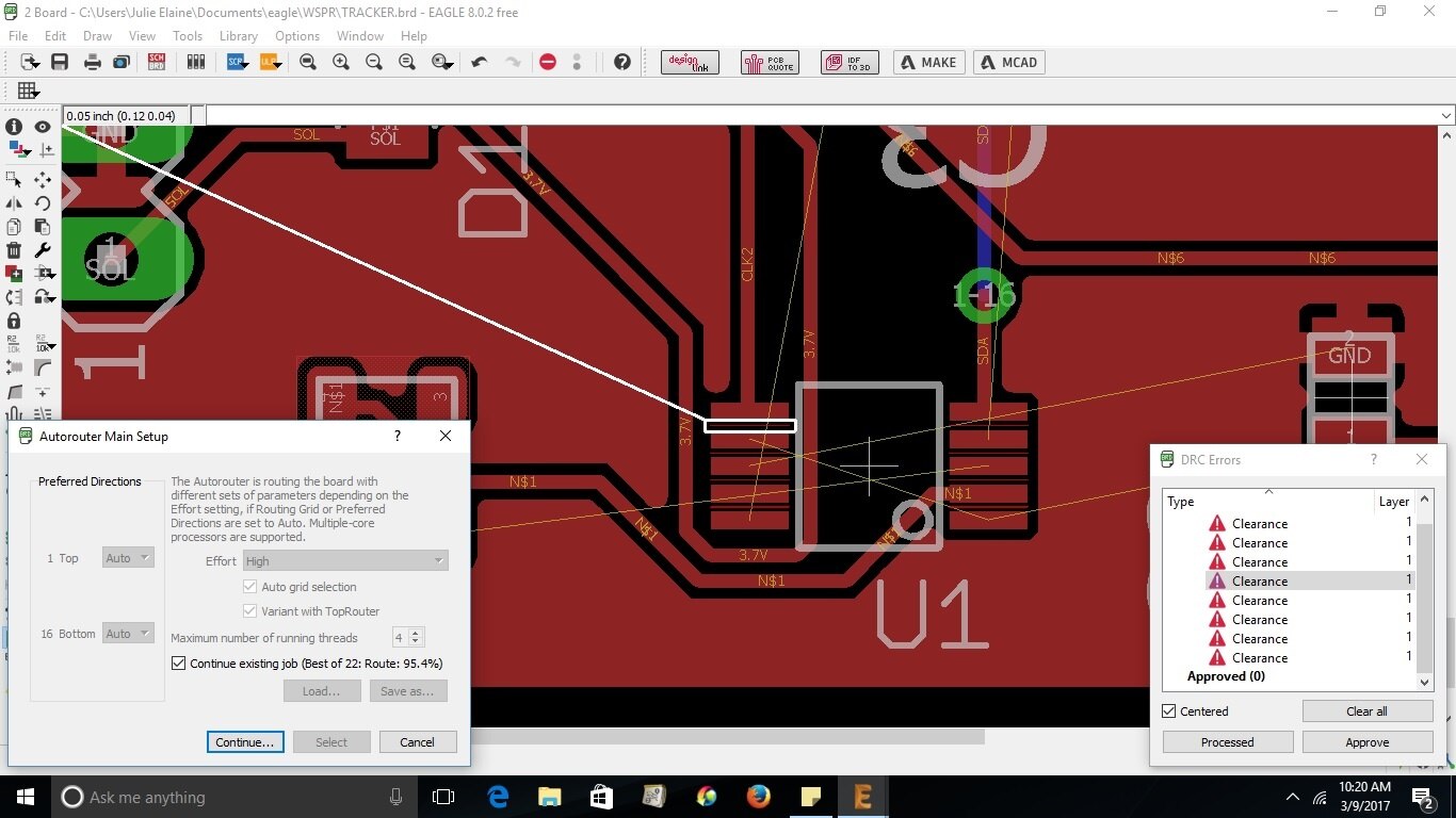
    Autorouting shows some connections bad.A run of the DRC once again shows the same issue regarding clearance on the Si5153a IC.

    I am am bit confused about auto routing since there are few options.This time,I set it up with EFFORT set to high rather than default.

    I still have a vague knowledge in where this should be anyhow.Still searching out more info.

    image

    • Cancel
    • Vote Up 0 Vote Down
    • Sign in to reply
    • Verify Answer
    • Cancel
  • n2nxz
    0 n2nxz over 9 years ago in reply to n2nxz

    Decided to try one more time tonight.

    This time I used the full size board work area without trying to squeeze everything in for a quick run.

    Also read this issue related - http://www.bot-thoughts.com/2013/09/eagle-sudden-clearance-errors-isolation.html

    Tried the solution in the post and also ran through my entire design rules settings.

    Whatever it was I get NO DRC errors now.

    Since I changed 3 major settings,not sure which it was causing my headaches.

    Tomorrow going to try rewriting the schematic the way I originally planned and shrink it down to a reasonable size.

    See what happens.

    Jim

    • Cancel
    • Vote Up 0 Vote Down
    • Sign in to reply
    • Verify Answer
    • Cancel
  • n2nxz
    0 n2nxz over 9 years ago in reply to rachaelp

    Just sharing to the group for the records on this topic.

    No hurry for me and do not expect anyone to solve my issues.I needed to walk away from it awhile and clear my head.

    Still waiting for the final components to arrive anyhow so will be some time before planning a build.

    I am sure someone with experience in Eagle will know what I am doing wrong...most likely the fact I need to just keep working on it and learn more.

    Jim

    • Cancel
    • Vote Up 0 Vote Down
    • Sign in to reply
    • Verify Answer
    • Cancel
  • rachaelp
    0 rachaelp over 9 years ago in reply to n2nxz

    Hi James,


    Sorry, I haven't been ignoring your posts, I've been out this evening. I'll take a look at what you've posted up in the morning :-)


    Best Regards,


    Rachael

    • Cancel
    • Vote Up 0 Vote Down
    • Sign in to reply
    • Verify Answer
    • Cancel
  • n2nxz
    0 n2nxz over 9 years ago in reply to n2nxz

    Another Si5351a library - Starting to Build my Personal EagleCAD Library — Tristan Robitaille

    • Cancel
    • Vote Up 0 Vote Down
    • Sign in to reply
    • Verify Answer
    • Cancel
  • n2nxz
    0 n2nxz over 9 years ago in reply to n2nxz

    Found another possibility for footprint - CAD/CAE Schematic Footprints and Symbols | Silicon Labs

    But another program to figure out to go with it .

    • Cancel
    • Vote Up 0 Vote Down
    • Sign in to reply
    • Verify Answer
    • Cancel
<>
element14 Community

element14 is the first online community specifically for engineers. Connect with your peers and get expert answers to your questions.

  • Members
  • Learn
  • Technologies
  • Challenges & Projects
  • Products
  • Store
  • About Us
  • Feedback & Support
  • FAQs
  • Terms of Use
  • Privacy Policy
  • Legal and Copyright Notices
  • Sitemap
  • Cookies

An Avnet Company © 2026 Premier Farnell Limited. All Rights Reserved.

Premier Farnell Ltd, registered in England and Wales (no 00876412), registered office: Farnell House, Forge Lane, Leeds LS12 2NE.

Follow element14

  • X
  • Facebook
  • linkedin
  • YouTube