element14 Community
element14 Community
    Register Log In
  • Site
  • Search
  • Log In Register
  • Community Hub
    Community Hub
    • What's New on element14
    • Feedback and Support
    • Benefits of Membership
    • Personal Blogs
    • Members Area
    • Achievement Levels
  • Learn
    Learn
    • Ask an Expert
    • eBooks
    • element14 presents
    • Learning Center
    • Tech Spotlight
    • STEM Academy
    • Webinars, Training and Events
    • Learning Groups
  • Technologies
    Technologies
    • 3D Printing
    • FPGA
    • Industrial Automation
    • Internet of Things
    • Power & Energy
    • Sensors
    • Technology Groups
  • Challenges & Projects
    Challenges & Projects
    • Design Challenges
    • element14 presents Projects
    • Project14
    • Arduino Projects
    • Raspberry Pi Projects
    • Project Groups
  • Products
    Products
    • Arduino
    • Avnet Boards Community
    • Dev Tools
    • Manufacturers
    • Multicomp Pro
    • Product Groups
    • Raspberry Pi
    • RoadTests & Reviews
  • About Us
  • Store
    Store
    • Visit Your Store
    • Choose another store...
      • Europe
      •  Austria (German)
      •  Belgium (Dutch, French)
      •  Bulgaria (Bulgarian)
      •  Czech Republic (Czech)
      •  Denmark (Danish)
      •  Estonia (Estonian)
      •  Finland (Finnish)
      •  France (French)
      •  Germany (German)
      •  Hungary (Hungarian)
      •  Ireland
      •  Israel
      •  Italy (Italian)
      •  Latvia (Latvian)
      •  
      •  Lithuania (Lithuanian)
      •  Netherlands (Dutch)
      •  Norway (Norwegian)
      •  Poland (Polish)
      •  Portugal (Portuguese)
      •  Romania (Romanian)
      •  Russia (Russian)
      •  Slovakia (Slovak)
      •  Slovenia (Slovenian)
      •  Spain (Spanish)
      •  Sweden (Swedish)
      •  Switzerland(German, French)
      •  Turkey (Turkish)
      •  United Kingdom
      • Asia Pacific
      •  Australia
      •  China
      •  Hong Kong
      •  India
      •  Korea (Korean)
      •  Malaysia
      •  New Zealand
      •  Philippines
      •  Singapore
      •  Taiwan
      •  Thailand (Thai)
      • Americas
      •  Brazil (Portuguese)
      •  Canada
      •  Mexico (Spanish)
      •  United States
      Can't find the country/region you're looking for? Visit our export site or find a local distributor.
  • Translate
  • Profile
  • Settings
Autodesk EAGLE
  • Products
  • More
Autodesk EAGLE
Forum Eagle smd-ipc.lbr footprints not quite right?
  • Blog
  • Forum
  • Documents
  • Events
  • Polls
  • Files
  • Members
  • Mentions
  • Sub-Groups
  • Tags
  • More
  • Cancel
  • New
Join Autodesk EAGLE to participate - click to join for free!
Actions
  • Share
  • More
  • Cancel
Forum Thread Details
  • State Verified Answer
  • Replies 3 replies
  • Subscribers 176 subscribers
  • Views 1706 views
  • Users 0 members are here
Related

Eagle smd-ipc.lbr footprints not quite right?

gandrewstone
gandrewstone over 6 years ago

Maybe I'm reading something wrong, but I think that certain footprints may be slightly off so I'd like a second opinion.


smd-ipc.lbr claims that it is based on IPC-SM-782.  I'm looking at that document from here:  https://www.pcb-3d.com/wordpress/wp-content/uploads/ipc-sm-782a_amendment_1_and_2.pdf


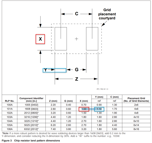
I'm working off of page 73 in the Surface Mount Design and Land Pattern Standard Chapter section 5.0 Land pattern dimensions.


When I read Figure 3, it looks like they've used the label "X" for the vertical pad size and "Y" for the horizontal size.  That's unintuitive... but the figure very clearly marks the dimensions.  And my drawn pads don't match up with smd-ipc.lbr for the 0603 part -- they match perfectly when the X and Y are transposed, so perhaps the smd-ipc.lbr author got confused with the X and Y labelling.


Can someone check my reading of this doc?


A lot of the other resistor footprints in smd-ipc.lbr are slightly different than this doc as well but not clearly transposed.  As we all know from experience, there is quite a bit of fudge in the pads of SMT resistors, which is probably why these footprints are generally working.  However, the doc is supposed to be the "best" (that is, providing the best yields) land pattern, so if fixing smd-ipc.lbr stops a few tombstones in everybody's runs that would be a worthy goal I think.  ... Or maybe the doc is obsolete and the smd-ipc dimensions are what is currently considered "best"?


Regards,

Andrew

  • Sign in to reply
  • Cancel
Parents
  • shabaz
    0 shabaz over 6 years ago

    Hi Andrew,


    The point you make regarding the size is true, it looks incorrect:

    image

    image

    However as Gerald says, it's better to confirm from the manufacturer's datasheet since they will have better guidelines (and production team experience with PCB manufacturers may also offer up guidelines).

    The error between swapping X and Y is small, (1x1.1 versus 1.1x1) and some datasheets specify an even bigger difference anyway, for their recommended pads

    e.g. Panasonic suggestion for their 0603 resistors:

    image

    • Cancel
    • Vote Up 0 Vote Down
    • Sign in to reply
    • Verify Answer
    • Reject Answer
    • Cancel
Reply
  • shabaz
    0 shabaz over 6 years ago

    Hi Andrew,


    The point you make regarding the size is true, it looks incorrect:

    image

    image

    However as Gerald says, it's better to confirm from the manufacturer's datasheet since they will have better guidelines (and production team experience with PCB manufacturers may also offer up guidelines).

    The error between swapping X and Y is small, (1x1.1 versus 1.1x1) and some datasheets specify an even bigger difference anyway, for their recommended pads

    e.g. Panasonic suggestion for their 0603 resistors:

    image

    • Cancel
    • Vote Up 0 Vote Down
    • Sign in to reply
    • Verify Answer
    • Reject Answer
    • Cancel
Children
No Data
element14 Community

element14 is the first online community specifically for engineers. Connect with your peers and get expert answers to your questions.

  • Members
  • Learn
  • Technologies
  • Challenges & Projects
  • Products
  • Store
  • About Us
  • Feedback & Support
  • FAQs
  • Terms of Use
  • Privacy Policy
  • Legal and Copyright Notices
  • Sitemap
  • Cookies

An Avnet Company © 2025 Premier Farnell Limited. All Rights Reserved.

Premier Farnell Ltd, registered in England and Wales (no 00876412), registered office: Farnell House, Forge Lane, Leeds LS12 2NE.

ICP 备案号 10220084.

Follow element14

  • X
  • Facebook
  • linkedin
  • YouTube