element14 Community
element14 Community
    Register Log In
  • Site
  • Search
  • Log In Register
  • Community Hub
    Community Hub
    • What's New on element14
    • Feedback and Support
    • Benefits of Membership
    • Personal Blogs
    • Members Area
    • Achievement Levels
  • Learn
    Learn
    • Ask an Expert
    • eBooks
    • element14 presents
    • Learning Center
    • Tech Spotlight
    • STEM Academy
    • Webinars, Training and Events
    • Learning Groups
  • Technologies
    Technologies
    • 3D Printing
    • FPGA
    • Industrial Automation
    • Internet of Things
    • Power & Energy
    • Sensors
    • Technology Groups
  • Challenges & Projects
    Challenges & Projects
    • Design Challenges
    • element14 presents Projects
    • Project14
    • Arduino Projects
    • Raspberry Pi Projects
    • Project Groups
  • Products
    Products
    • Arduino
    • Avnet & Tria Boards Community
    • Dev Tools
    • Manufacturers
    • Multicomp Pro
    • Product Groups
    • Raspberry Pi
    • RoadTests & Reviews
  • About Us
  • Store
    Store
    • Visit Your Store
    • Choose another store...
      • Europe
      •  Austria (German)
      •  Belgium (Dutch, French)
      •  Bulgaria (Bulgarian)
      •  Czech Republic (Czech)
      •  Denmark (Danish)
      •  Estonia (Estonian)
      •  Finland (Finnish)
      •  France (French)
      •  Germany (German)
      •  Hungary (Hungarian)
      •  Ireland
      •  Israel
      •  Italy (Italian)
      •  Latvia (Latvian)
      •  
      •  Lithuania (Lithuanian)
      •  Netherlands (Dutch)
      •  Norway (Norwegian)
      •  Poland (Polish)
      •  Portugal (Portuguese)
      •  Romania (Romanian)
      •  Russia (Russian)
      •  Slovakia (Slovak)
      •  Slovenia (Slovenian)
      •  Spain (Spanish)
      •  Sweden (Swedish)
      •  Switzerland(German, French)
      •  Turkey (Turkish)
      •  United Kingdom
      • Asia Pacific
      •  Australia
      •  China
      •  Hong Kong
      •  India
      •  Korea (Korean)
      •  Malaysia
      •  New Zealand
      •  Philippines
      •  Singapore
      •  Taiwan
      •  Thailand (Thai)
      • Americas
      •  Brazil (Portuguese)
      •  Canada
      •  Mexico (Spanish)
      •  United States
      Can't find the country/region you're looking for? Visit our export site or find a local distributor.
  • Translate
  • Profile
  • Settings
Autodesk EAGLE
  • Products
  • More
Autodesk EAGLE
Forum Questions on PCB manufacture
  • Blog
  • Forum
  • Documents
  • Events
  • Polls
  • Files
  • Members
  • Mentions
  • Sub-Groups
  • Tags
  • More
  • Cancel
  • New
Join Autodesk EAGLE to participate - click to join for free!
Actions
  • Share
  • More
  • Cancel
Forum Thread Details
  • State Not Answered
  • Replies 2 replies
  • Subscribers 176 subscribers
  • Views 354 views
  • Users 0 members are here
Related

Questions on PCB manufacture

Former Member
Former Member over 12 years ago

Hi all,


I am close to getting my PCB manufactured, however I have a few questions to ask regarding my board.


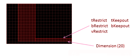
It mentions in manual (V6, page 281) that you should leave 2mm free of Copper around the edge of the board.  I have done a Copper pour (ratsnest command) for top and bottom layers, and the gap is 50 mil not 80 mil - how do I change this to 80 mil?


Page 281 also mentions identifying Component side and bottom side with CS and BS.  I have done this on layers 1 and 16, but when I run DRC it comes up with 2 errors:  No real vector font, and Width.


Finally how do I apply Fiducial marks to the board? 


Hope to hear from you soon,


Cheers,


Osman.

  • Sign in to reply
  • Cancel

Top Replies

  • Richard_H
    Richard_H over 12 years ago +1
    Hi, texts in copper layers should be writeen in vector font. That's a property of the text you can adjust. I suppose you used proportional font and this will result in a different view on the board after…
Parents
  • shabaz
    0 shabaz over 12 years ago

    Hi Osman,


    You are likely fine with your 50mil gap; many manufacturers can handle a much lower gap than that too. Normally the way to do it would have been to have had 5 limits drawn on the edge of the board - t/b/vRestrict and t/bKeepout. The example below shows a corner of a board, with a wider gap on the left side of the board (where it was to slide into metal slots in an enclosure) and a narrower gap at the bottom of the board, for example. Not sure what the vector font issue is (I've not encountered it) but I just place normal text on the board, e.g. a copyright notice. For fiducial marks, you could create a component, or just draw circles on the copper layers, and a slightly larger circle on the t/bStop layers. It's not needed for a hand-assembled board of course. The PCB manufacturer does not need it.


    image

    • Cancel
    • Vote Up 0 Vote Down
    • Sign in to reply
    • Verify Answer
    • Cancel
Reply
  • shabaz
    0 shabaz over 12 years ago

    Hi Osman,


    You are likely fine with your 50mil gap; many manufacturers can handle a much lower gap than that too. Normally the way to do it would have been to have had 5 limits drawn on the edge of the board - t/b/vRestrict and t/bKeepout. The example below shows a corner of a board, with a wider gap on the left side of the board (where it was to slide into metal slots in an enclosure) and a narrower gap at the bottom of the board, for example. Not sure what the vector font issue is (I've not encountered it) but I just place normal text on the board, e.g. a copyright notice. For fiducial marks, you could create a component, or just draw circles on the copper layers, and a slightly larger circle on the t/bStop layers. It's not needed for a hand-assembled board of course. The PCB manufacturer does not need it.


    image

    • Cancel
    • Vote Up 0 Vote Down
    • Sign in to reply
    • Verify Answer
    • Cancel
Children
No Data
element14 Community

element14 is the first online community specifically for engineers. Connect with your peers and get expert answers to your questions.

  • Members
  • Learn
  • Technologies
  • Challenges & Projects
  • Products
  • Store
  • About Us
  • Feedback & Support
  • FAQs
  • Terms of Use
  • Privacy Policy
  • Legal and Copyright Notices
  • Sitemap
  • Cookies

An Avnet Company © 2025 Premier Farnell Limited. All Rights Reserved.

Premier Farnell Ltd, registered in England and Wales (no 00876412), registered office: Farnell House, Forge Lane, Leeds LS12 2NE.

ICP 备案号 10220084.

Follow element14

  • X
  • Facebook
  • linkedin
  • YouTube