

Hi,
I'm working on a fairly general procedure for laying out stripboard (Veroboard) designs using the schematic editor, without designing a board (see post of 2nd February). It looks as though it can be done and you can still create a net. The net traces will use the copper when they go along the strips, and be thought of as jumpers elsewhere (a schematic has only one side).
The stripboard, holes, track cuts and points to be soldered are created as "pinless" library devices and placed on separate layers. The library has a set of component devices where the symbols have the same dimensions as the packages.
The only remaining difficulty is that if I follow the manual to the letter, it isn't possible to allow the jumpers to get closer than 0.1 inch to each other, and that takes a lot of space.
The manual warns of dire consequences if you don't restrict yourself to the 0.1 inch grid when drawing schematics.
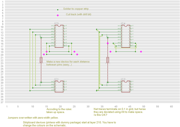
My question is whether it would be "safe" to move segments of the net traces off grid using Alt, provided the traces begin and end on grid points. The image shows what I'd like to do. This doesn't matter at all if you will never need to use the net, but I want to be absolutely sure before publishing anything.
