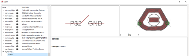
hi,
I really facing difficulties creating a library for this component. can someone help please?
here is a link to the datasheet https://files.elv.com/Assets/Produkte/2/243/24380/Downloads/24380_TDW_data.pdf
its a triangle metal dome switch
thanks
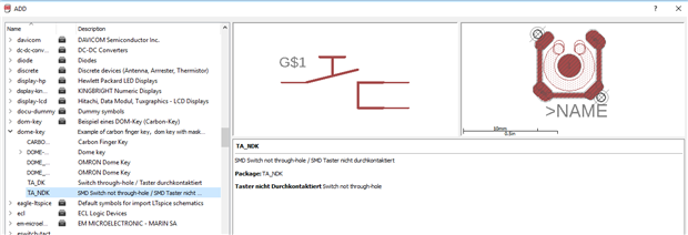
hi,
I really facing difficulties creating a library for this component. can someone help please?
here is a link to the datasheet https://files.elv.com/Assets/Produkte/2/243/24380/Downloads/24380_TDW_data.pdf
its a triangle metal dome switch
thanks