element14 Community
element14 Community
    Register Log In
  • Site
  • Search
  • Log In Register
  • Community Hub
    Community Hub
    • What's New on element14
    • Feedback and Support
    • Benefits of Membership
    • Personal Blogs
    • Members Area
    • Achievement Levels
  • Learn
    Learn
    • Ask an Expert
    • eBooks
    • element14 presents
    • Learning Center
    • Tech Spotlight
    • STEM Academy
    • Webinars, Training and Events
    • Learning Groups
  • Technologies
    Technologies
    • 3D Printing
    • FPGA
    • Industrial Automation
    • Internet of Things
    • Power & Energy
    • Sensors
    • Technology Groups
  • Challenges & Projects
    Challenges & Projects
    • Design Challenges
    • element14 presents Projects
    • Project14
    • Arduino Projects
    • Raspberry Pi Projects
    • Project Groups
  • Products
    Products
    • Arduino
    • Avnet Boards Community
    • Dev Tools
    • Manufacturers
    • Multicomp Pro
    • Product Groups
    • Raspberry Pi
    • RoadTests & Reviews
  • About Us
  • Store
    Store
    • Visit Your Store
    • Choose another store...
      • Europe
      •  Austria (German)
      •  Belgium (Dutch, French)
      •  Bulgaria (Bulgarian)
      •  Czech Republic (Czech)
      •  Denmark (Danish)
      •  Estonia (Estonian)
      •  Finland (Finnish)
      •  France (French)
      •  Germany (German)
      •  Hungary (Hungarian)
      •  Ireland
      •  Israel
      •  Italy (Italian)
      •  Latvia (Latvian)
      •  
      •  Lithuania (Lithuanian)
      •  Netherlands (Dutch)
      •  Norway (Norwegian)
      •  Poland (Polish)
      •  Portugal (Portuguese)
      •  Romania (Romanian)
      •  Russia (Russian)
      •  Slovakia (Slovak)
      •  Slovenia (Slovenian)
      •  Spain (Spanish)
      •  Sweden (Swedish)
      •  Switzerland(German, French)
      •  Turkey (Turkish)
      •  United Kingdom
      • Asia Pacific
      •  Australia
      •  China
      •  Hong Kong
      •  India
      •  Korea (Korean)
      •  Malaysia
      •  New Zealand
      •  Philippines
      •  Singapore
      •  Taiwan
      •  Thailand (Thai)
      • Americas
      •  Brazil (Portuguese)
      •  Canada
      •  Mexico (Spanish)
      •  United States
      Can't find the country/region you're looking for? Visit our export site or find a local distributor.
  • Translate
  • Profile
  • Settings
Autodesk EAGLE
  • Products
  • More
Autodesk EAGLE
Forum help with PCB layout checking
  • Blog
  • Forum
  • Documents
  • Events
  • Polls
  • Files
  • Members
  • Mentions
  • Sub-Groups
  • Tags
  • More
  • Cancel
  • New
Join Autodesk EAGLE to participate - click to join for free!
Actions
  • Share
  • More
  • Cancel
Forum Thread Details
  • Replies 4 replies
  • Subscribers 177 subscribers
  • Views 1252 views
  • Users 0 members are here
Related

help with PCB layout checking

houandreas
houandreas over 7 years ago

images uploaded.

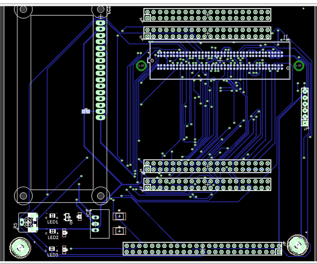
hi, with your help I finally finished my first board in eagle. But I don't have any experience before, so there might be some mistakes to fix. Here I upload my board and schematic files in my google drive. If anyone could help me with this would be so appreciated.

https://drive.google.com/open?id=1Cm6o7Ets-rg0RCMyVHRzhi6eLX1H9t_D

This board is an adapter board for video signal processing. So it's running high frequcency signals I guess(pixel time 40ns). I read a lot about it but it's more than I can handle for now...

And the placement of those components is quite limited, that is already the best placement I can do. I used autorouter so there is no DRC error for now (I apply the default DRC setting).

here are some net settings for this board, you can also see it in eagle.

signal trace width 10mil, Via 15mil, clearance 10mil.

Power trace width 20mil, Via 20mil. clearance 10mil.

I cannot route if trace width is wider since the LPC connector pins are so close to each other. But this should be enough. Later I will make top and bottom as ground plane and add some via,but now is too late...Again thank you image

imageimageimage

  • Sign in to reply
  • Cancel

Top Replies

  • shabaz
    shabaz over 7 years ago +4
    Hi Bin, There are many rich editor tools for presenting your design, such as inserting images inline, and even video.. You'll get more eyes looking at your question if the images are resized nicely and…
  • shabaz
    shabaz over 7 years ago +2
    Hi Bin, After using the autorouter, the DRC check still needs to be done, it cannot be assumed that it will do it for you (it doesn't as far as I understand, but I don't use the autorouter so Im not sure…
  • snidhi
    snidhi over 7 years ago +2
    yes I will agree to to the previous comments. DRC checks are very very important to run and understand even. Try to read through the DRC options and understand them with Eagle HELP. Some other cautionary…
Parents
  • snidhi
    snidhi over 7 years ago

    yes I will agree to to the previous comments.


    DRC checks are very very important to run and understand even. Try to read through the DRC options and understand them with Eagle HELP.


    Some other cautionary measures that I often take are

    • Look for GND islands or big cut outs in the GND and power planes (for internal and external layers). Specially if there is any impedance controlled lines I would make sure there is appropriate GND planes above and below them.
    • Use enough stitching vias on the board.
    • Make sure the traces are not too close together to avoid some basic cross talk issues. Only applicable for critical signal lines.
    • Re-check the Gerbers for proper solder mask solder stop layers.


    Cheers image

    • Cancel
    • Vote Up +2 Vote Down
    • Sign in to reply
    • Cancel
Reply
  • snidhi
    snidhi over 7 years ago

    yes I will agree to to the previous comments.


    DRC checks are very very important to run and understand even. Try to read through the DRC options and understand them with Eagle HELP.


    Some other cautionary measures that I often take are

    • Look for GND islands or big cut outs in the GND and power planes (for internal and external layers). Specially if there is any impedance controlled lines I would make sure there is appropriate GND planes above and below them.
    • Use enough stitching vias on the board.
    • Make sure the traces are not too close together to avoid some basic cross talk issues. Only applicable for critical signal lines.
    • Re-check the Gerbers for proper solder mask solder stop layers.


    Cheers image

    • Cancel
    • Vote Up +2 Vote Down
    • Sign in to reply
    • Cancel
Children
No Data
element14 Community

element14 is the first online community specifically for engineers. Connect with your peers and get expert answers to your questions.

  • Members
  • Learn
  • Technologies
  • Challenges & Projects
  • Products
  • Store
  • About Us
  • Feedback & Support
  • FAQs
  • Terms of Use
  • Privacy Policy
  • Legal and Copyright Notices
  • Sitemap
  • Cookies

An Avnet Company © 2025 Premier Farnell Limited. All Rights Reserved.

Premier Farnell Ltd, registered in England and Wales (no 00876412), registered office: Farnell House, Forge Lane, Leeds LS12 2NE.

ICP 备案号 10220084.

Follow element14

  • X
  • Facebook
  • linkedin
  • YouTube