element14 Community
element14 Community
    Register Log In
  • Site
  • Search
  • Log In Register
  • About Us
  • Community Hub
    Community Hub
    • What's New on element14
    • Feedback and Support
    • Benefits of Membership
    • Personal Blogs
    • Members Area
    • Achievement Levels
  • Learn
    Learn
    • Ask an Expert
    • eBooks
    • element14 presents
    • Learning Center
    • Tech Spotlight
    • STEM Academy
    • Webinars, Training and Events
    • Learning Groups
  • Technologies
    Technologies
    • 3D Printing
    • FPGA
    • Industrial Automation
    • Internet of Things
    • Power & Energy
    • Sensors
    • Technology Groups
  • Challenges & Projects
    Challenges & Projects
    • Design Challenges
    • element14 presents Projects
    • Project14
    • Arduino Projects
    • Raspberry Pi Projects
    • Project Groups
  • Products
    Products
    • Arduino
    • Avnet Boards Community
    • Dev Tools
    • Manufacturers
    • Multicomp Pro
    • Product Groups
    • Raspberry Pi
    • RoadTests & Reviews
  • Store
    Store
    • Visit Your Store
    • Choose another store...
      • Europe
      •  Austria (German)
      •  Belgium (Dutch, French)
      •  Bulgaria (Bulgarian)
      •  Czech Republic (Czech)
      •  Denmark (Danish)
      •  Estonia (Estonian)
      •  Finland (Finnish)
      •  France (French)
      •  Germany (German)
      •  Hungary (Hungarian)
      •  Ireland
      •  Israel
      •  Italy (Italian)
      •  Latvia (Latvian)
      •  
      •  Lithuania (Lithuanian)
      •  Netherlands (Dutch)
      •  Norway (Norwegian)
      •  Poland (Polish)
      •  Portugal (Portuguese)
      •  Romania (Romanian)
      •  Russia (Russian)
      •  Slovakia (Slovak)
      •  Slovenia (Slovenian)
      •  Spain (Spanish)
      •  Sweden (Swedish)
      •  Switzerland(German, French)
      •  Turkey (Turkish)
      •  United Kingdom
      • Asia Pacific
      •  Australia
      •  China
      •  Hong Kong
      •  India
      •  Korea (Korean)
      •  Malaysia
      •  New Zealand
      •  Philippines
      •  Singapore
      •  Taiwan
      •  Thailand (Thai)
      • Americas
      •  Brazil (Portuguese)
      •  Canada
      •  Mexico (Spanish)
      •  United States
      Can't find the country/region you're looking for? Visit our export site or find a local distributor.
  • Translate
  • Profile
  • Settings
Autodesk EAGLE
  • Products
  • More
Autodesk EAGLE
Documents How to Set a 4 Layers PCB in EAGLE
  • Blog
  • Forum
  • Documents
  • Events
  • Polls
  • Files
  • Members
  • Mentions
  • Sub-Groups
  • Tags
  • More
  • Cancel
  • New
Join Autodesk EAGLE to participate - click to join for free!
Actions
  • Share
  • More
  • Cancel
Engagement
  • Author Author: Oliver
  • Date Created: 28 Jan 2011 9:30 AM Date Created
  • Last Updated Last Updated: 7 Oct 2021 7:52 AM
  • Views 1730 views
  • Likes 0 likes
  • Comments 1 comment
Related
Recommended

How to Set a 4 Layers PCB in EAGLE

用EAGLE软件设计多层电路板(4层为例),需要进行以下设置,请检查您的设置是否正确?
 
下面以EAGLE自带的例子singlesided.brd来演示(尽管名字是单层版,但是同样可以设置为4层电路板)

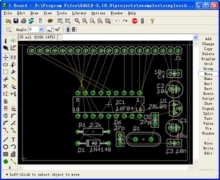
1.    首先打开singlesided.brd文件,将影响视觉的第41层tRestrick关闭(使用display命令),可以看到下面的图片:

image

2.    点击Edit菜单下面的“Design rules…”打开Design Rules设置界面,并选择Layers标签,如下图所示,

image

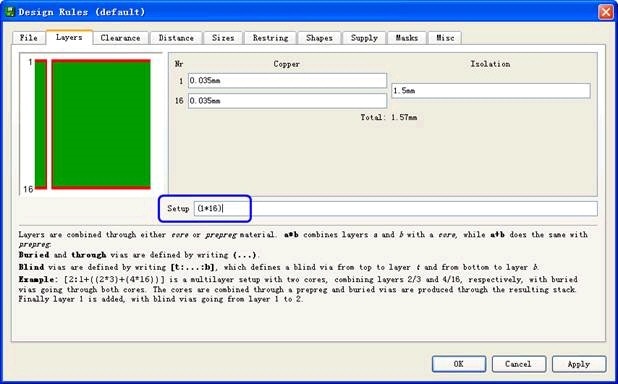
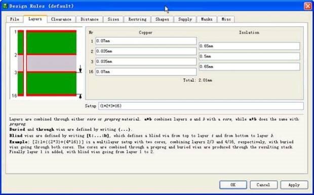
3.   在上图Setup(图上的蓝色方框)处将2层电路板设置为4层,将(1*16)更改为(1*2+3*16),可以看到左边的图层示意已经变成4层。修改自己需要的copper和isolation厚度,比如:外层敷铜厚度2oz(70um),内层敷铜厚度1oz(35um),再更改绝缘层厚度,使得总的层厚度为2mm。得到如下图示内容(具体的敷铜层厚度和PCB板厚请和您的PCB制造商联系,本处仅仅是示意),后面的Restring,Supply等标签可以根据需要修改,此处用系统默认值。最后点击OK

image

通过前面的操作,我们已经将电路板设置为4层了,下面的操作是将中间层定义为supply layer,即电源层和地层,并分配网络。

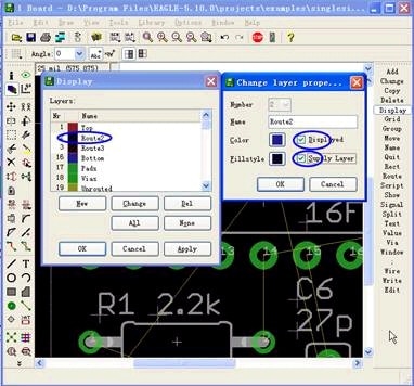
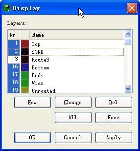
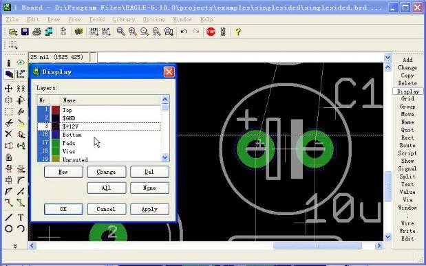
4.   使用Display命令打开Display窗口,如下图所示,可以看到我们添加的layer2和layer3出现了(有可能在最后出现,请下拉滚动条),选中layer2 (Route2),点击下面的Change按钮,在打开的窗口中选中Displayed和Supply Layer (打勾),并将Route2改成GND,颜色默认,然后点击OK返回,可以看到在GND的前面多了个符号“$”,

imageimage


5.   点击OK关闭上图Display窗口,可以看到在通孔焊盘外边会出现一圈蓝色阴影,这表示地层已经设置,如下图所示:

image

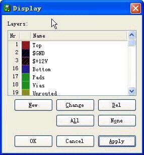
6.   同样的操作再选择Layer3,改Route3名为+12V (由于该PCB图中没有Power或者VCC等网络,我们选择+12V作为电源层网络名称),勾选Displayed和Power Layer,点击OK关闭Display窗口,如下图所示:

image

自此,我们已经完成将PCB板设置为4层的所有操作,下面将是如何确认我们的PCB会是4层显示:

7.   请确保您所设计的4层板中需要将什么网络放到电源层和地层,本例中我将GND和+12V分别放到地层和电源层,因此我将Layer命名为GND,Layer3命名为+12V。仔细看下图中我关闭GND层并且打开+12V层的效果,右边电解电容C1的正端有一个热焊盘,这表示该电容的正极在电源层有连接;负端是实心的隔离层,表示电容负极在电源层是不会产生连接的。

image


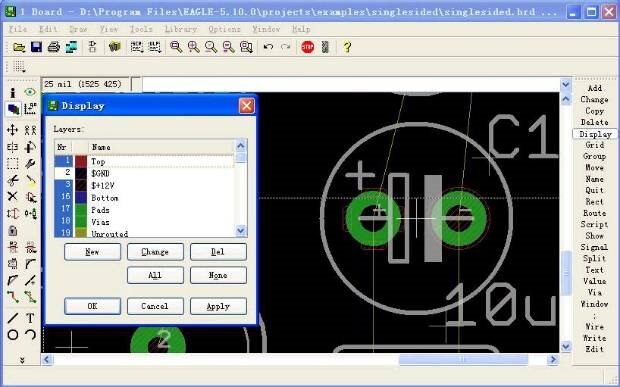
下图为我关闭+12V层并且打开GND层的效果,右边电解电容C1的负端有一个热焊盘,这表示该电容的负极在地层有连接;正端是实心的隔离层,表示电容正极在地层是不会产生连接的。热焊盘的参数设置请在Design rules的设置窗口中Supply标签处设置。

image


最后请注意:

EAGLE和所有其他电子设计软件一样,是用负片产生电源层和地层Gerber数据,因此您在设计环境中看到的和真正的Gerber产生的数据相反。

和其他的EDA软件类似,如果要使用负片产生电源层和地层数据,需要在电源层和地层的PCB边缘使用大约50mil的非电气连接线画一个封闭的形状,这样做的目的是使电源层和地层产生的敷铜区不会到达PCB的边缘,在PCB切割时不会产生铜屑造成短路,并且避免信号在电路板边缘产生射频干扰。


切忌!切忌!!!!!!!

  • eagle
  • pcb_layout
  • 4_layer
  • design_rules
  • cadsoft
  • Share
  • History
  • More
  • Cancel
  • Sign in to reply
  • huayuliang
    huayuliang over 14 years ago

    十分感谢。

    • Cancel
    • Vote Up 0 Vote Down
    • Sign in to reply
    • More
    • Cancel
element14 Community

element14 is the first online community specifically for engineers. Connect with your peers and get expert answers to your questions.

  • Members
  • Learn
  • Technologies
  • Challenges & Projects
  • Products
  • Store
  • About Us
  • Feedback & Support
  • FAQs
  • Terms of Use
  • Privacy Policy
  • Legal and Copyright Notices
  • Sitemap
  • Cookies

An Avnet Company © 2025 Premier Farnell Limited. All Rights Reserved.

Premier Farnell Ltd, registered in England and Wales (no 00876412), registered office: Farnell House, Forge Lane, Leeds LS12 2NE.

ICP 备案号 10220084.

Follow element14

  • X
  • Facebook
  • linkedin
  • YouTube