element14 Community
element14 Community
    Register Log In
  • Site
  • Search
  • Log In Register
  • Community Hub
    Community Hub
    • What's New on element14
    • Feedback and Support
    • Benefits of Membership
    • Personal Blogs
    • Members Area
    • Achievement Levels
  • Learn
    Learn
    • Ask an Expert
    • eBooks
    • element14 presents
    • Learning Center
    • Tech Spotlight
    • STEM Academy
    • Webinars, Training and Events
    • Learning Groups
  • Technologies
    Technologies
    • 3D Printing
    • FPGA
    • Industrial Automation
    • Internet of Things
    • Power & Energy
    • Sensors
    • Technology Groups
  • Challenges & Projects
    Challenges & Projects
    • Design Challenges
    • element14 presents Projects
    • Project14
    • Arduino Projects
    • Raspberry Pi Projects
    • Project Groups
  • Products
    Products
    • Arduino
    • Avnet Boards Community
    • Dev Tools
    • Manufacturers
    • Multicomp Pro
    • Product Groups
    • Raspberry Pi
    • RoadTests & Reviews
  • About Us
  • Store
    Store
    • Visit Your Store
    • Choose another store...
      • Europe
      •  Austria (German)
      •  Belgium (Dutch, French)
      •  Bulgaria (Bulgarian)
      •  Czech Republic (Czech)
      •  Denmark (Danish)
      •  Estonia (Estonian)
      •  Finland (Finnish)
      •  France (French)
      •  Germany (German)
      •  Hungary (Hungarian)
      •  Ireland
      •  Israel
      •  Italy (Italian)
      •  Latvia (Latvian)
      •  
      •  Lithuania (Lithuanian)
      •  Netherlands (Dutch)
      •  Norway (Norwegian)
      •  Poland (Polish)
      •  Portugal (Portuguese)
      •  Romania (Romanian)
      •  Russia (Russian)
      •  Slovakia (Slovak)
      •  Slovenia (Slovenian)
      •  Spain (Spanish)
      •  Sweden (Swedish)
      •  Switzerland(German, French)
      •  Turkey (Turkish)
      •  United Kingdom
      • Asia Pacific
      •  Australia
      •  China
      •  Hong Kong
      •  India
      •  Korea (Korean)
      •  Malaysia
      •  New Zealand
      •  Philippines
      •  Singapore
      •  Taiwan
      •  Thailand (Thai)
      • Americas
      •  Brazil (Portuguese)
      •  Canada
      •  Mexico (Spanish)
      •  United States
      Can't find the country/region you're looking for? Visit our export site or find a local distributor.
  • Translate
  • Profile
  • Settings
Altium CircuitStudio
  • Products
  • Manufacturers
  • Altium CircuitStudio
  • More
  • Cancel
Altium CircuitStudio
Blog Part-3: Generate output files for printing – Eureka!!
  • Blog
  • Forum
  • Documents
  • Events
  • Polls
  • Members
  • Mentions
  • Sub-Groups
  • Tags
  • More
  • Cancel
  • New
Join Altium CircuitStudio to participate - click to join for free!
  • Share
  • More
  • Cancel
Group Actions
  • Group RSS
  • More
  • Cancel
Engagement
  • Author Author: AshokRao
  • Date Created: 11 May 2016 10:14 AM Date Created
  • Views 802 views
  • Likes 0 likes
  • Comments 0 comments
  • getting started with altium circuit studio
  • circuit studio
  • pcb design
Related
Recommended

Part-3: Generate output files for printing – Eureka!!

AshokRao
AshokRao
11 May 2016

Related Content:

Part 1:Create a schematic from your idea – Out of the head, into the tool.

Part 2: Make the PCB from your design – Almost there...

Part-3: Generate output files for printing – Eureka!!


Again, a reminder, if you still don't have your trial license, get it from here:

Professional PCB design tool | CircuitStudio


Right, after following Parts 1 & 2 of this blog series, you should have your design laid out and ready to print. However, no project proceeds without having any errors. In the previous parts, we compiled our design against the rules we set. But, are these fit for manufacturing? Let’s find out..


With your PCB document selected, navigate to Home → Design Rules →Design Rule Check as below. And click on “Run Design Rule Check...”

image

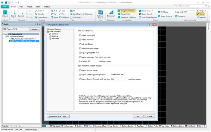
The Design Rule checker will validate your design against the rules set out and produce a report with all the violations. This is shown below:


image

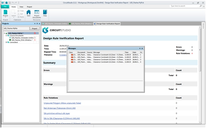
Close the “Messages” window and scroll down to the appropriate section in the report where the errors are listed. My rule violations are in the “clearance constraints” set under “Design Rules”.

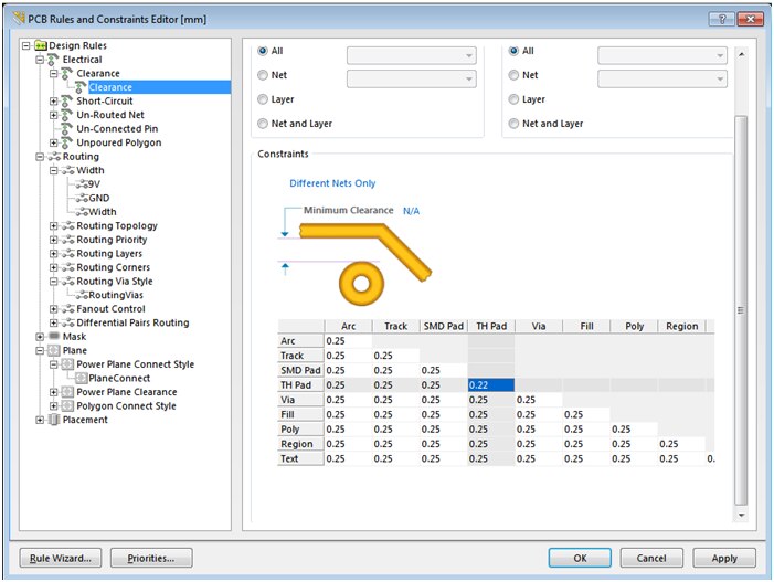
So, how do we fix it? Change the design rules..ha ha ha!!


With your PCB document selected, navigate to Home → Design Rules. Select the “Clearance” rule under “Electrial” section. Reduce the TH Pad to have a min clearance of 0.22mm as shown below and then click on “Apply” →”OK”.

image

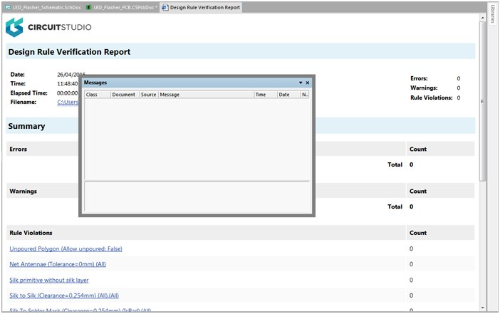
Now, run the “Design Rule Check” again as described above and your violations should have disappeared as shown below. Note the 0 rule violations.

image

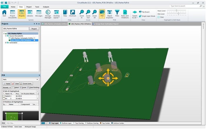
Save your project and move on to visualising your board in 3D.

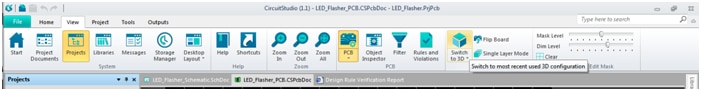
Click on the “View” tab and under “View” group in the ribbon menu, click on “Switch to 3D”.

image

With the mouse pointer on any component, hold the “Shift” key on the keyboard. You will see a 3D sphere on the component as below. With the shift key pressed, hold the right click and drag around the board to view it in 3D.

image

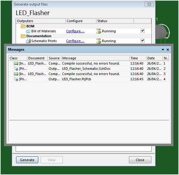
When you are happy, it’s time to generate the output files for the PCB manufacture. Navigate to the “Project” tab and click on “Generate Outputs”. You should see a window with all the output files that will be generated for the project like this below:

image

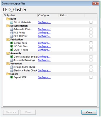
Click on the check boxes next to the ones you want to generate and then click on the “Generate” button at the bottom of the window.

image

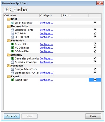
After a few minutes of waiting, the files will be generated. Save the files to a convenient location on your hard disk.

image

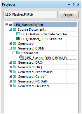
Notice in the “Projects” window there are now a lot of different documents specific to the project such as BOM, DRC, STEP, Drill/Pick Place etc for you to take them to the printer. Have a peek into each of these files (if you have the right viewers). The BOM is shown as an excel workbook for you to print/save etc as shown below.

image

From here on..you’re on your own soldier. Get those designs rolling. Have fun with Circuit Studio!


Further information from the e14 design center here:

https://www.element14.com/community/docs/DOC-73745?ICID=designctr-devtools-info

  • Sign in to reply
element14 Community

element14 is the first online community specifically for engineers. Connect with your peers and get expert answers to your questions.

  • Members
  • Learn
  • Technologies
  • Challenges & Projects
  • Products
  • Store
  • About Us
  • Feedback & Support
  • FAQs
  • Terms of Use
  • Privacy Policy
  • Legal and Copyright Notices
  • Sitemap
  • Cookies

An Avnet Company © 2025 Premier Farnell Limited. All Rights Reserved.

Premier Farnell Ltd, registered in England and Wales (no 00876412), registered office: Farnell House, Forge Lane, Leeds LS12 2NE.

ICP 备案号 10220084.

Follow element14

  • X
  • Facebook
  • linkedin
  • YouTube