Hi,
I would like to know if there is a solution to remove the varnish mask on a part of a track on circuit studio ?
I have not enough place to make the track at the right size so I need to solder a wire on the track.
Thanks
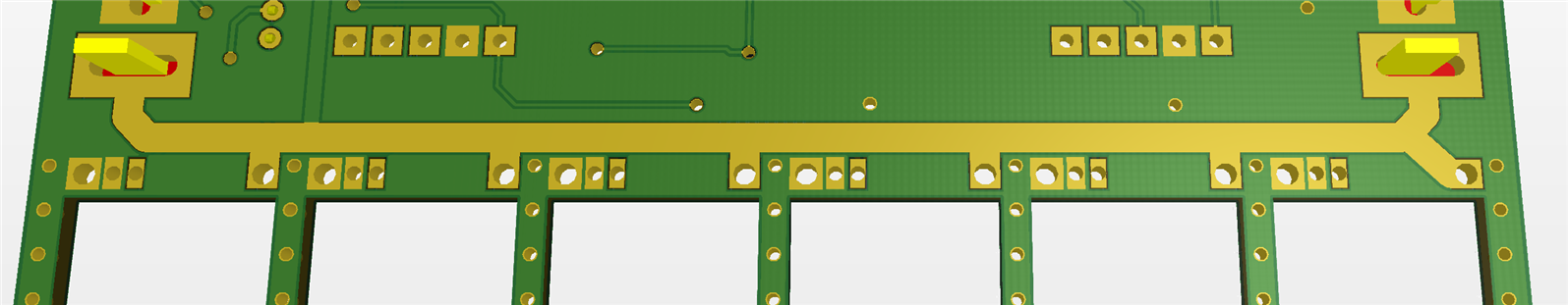
Hi,
I would like to know if there is a solution to remove the varnish mask on a part of a track on circuit studio ?
I have not enough place to make the track at the right size so I need to solder a wire on the track.
Thanks