element14 Community
element14 Community
    Register Log In
  • Site
  • Search
  • Log In Register
  • Community Hub
    Community Hub
    • What's New on element14
    • Feedback and Support
    • Benefits of Membership
    • Personal Blogs
    • Members Area
    • Achievement Levels
  • Learn
    Learn
    • Ask an Expert
    • eBooks
    • element14 presents
    • Learning Center
    • Tech Spotlight
    • STEM Academy
    • Webinars, Training and Events
    • Learning Groups
  • Technologies
    Technologies
    • 3D Printing
    • FPGA
    • Industrial Automation
    • Internet of Things
    • Power & Energy
    • Sensors
    • Technology Groups
  • Challenges & Projects
    Challenges & Projects
    • Design Challenges
    • element14 presents Projects
    • Project14
    • Arduino Projects
    • Raspberry Pi Projects
    • Project Groups
  • Products
    Products
    • Arduino
    • Avnet & Tria Boards Community
    • Dev Tools
    • Manufacturers
    • Multicomp Pro
    • Product Groups
    • Raspberry Pi
    • RoadTests & Reviews
  • About Us
  • Store
    Store
    • Visit Your Store
    • Choose another store...
      • Europe
      •  Austria (German)
      •  Belgium (Dutch, French)
      •  Bulgaria (Bulgarian)
      •  Czech Republic (Czech)
      •  Denmark (Danish)
      •  Estonia (Estonian)
      •  Finland (Finnish)
      •  France (French)
      •  Germany (German)
      •  Hungary (Hungarian)
      •  Ireland
      •  Israel
      •  Italy (Italian)
      •  Latvia (Latvian)
      •  
      •  Lithuania (Lithuanian)
      •  Netherlands (Dutch)
      •  Norway (Norwegian)
      •  Poland (Polish)
      •  Portugal (Portuguese)
      •  Romania (Romanian)
      •  Russia (Russian)
      •  Slovakia (Slovak)
      •  Slovenia (Slovenian)
      •  Spain (Spanish)
      •  Sweden (Swedish)
      •  Switzerland(German, French)
      •  Turkey (Turkish)
      •  United Kingdom
      • Asia Pacific
      •  Australia
      •  China
      •  Hong Kong
      •  India
      • Japan
      •  Korea (Korean)
      •  Malaysia
      •  New Zealand
      •  Philippines
      •  Singapore
      •  Taiwan
      •  Thailand (Thai)
      • Vietnam
      • Americas
      •  Brazil (Portuguese)
      •  Canada
      •  Mexico (Spanish)
      •  United States
      Can't find the country/region you're looking for? Visit our export site or find a local distributor.
  • Translate
  • Profile
  • Settings
Altium CircuitStudio
  • Products
  • Manufacturers
  • Altium CircuitStudio
  • More
  • Cancel
Altium CircuitStudio
Altium CircuitStudio Forum VMake via export in Gerbers with Solder mask over them
  • Blog
  • Forum
  • Documents
  • Events
  • Polls
  • Members
  • Mentions
  • Sub-Groups
  • Tags
  • More
  • Cancel
  • New
Join Altium CircuitStudio to participate - click to join for free!
Actions
  • Share
  • More
  • Cancel
Forum Thread Details
  • Locked Locked
  • Replies 4 replies
  • Subscribers 89 subscribers
  • Views 705 views
  • Users 0 members are here
Related
This discussion has been locked.
You can no longer post new replies to this discussion. If you have a question you can start a new discussion

VMake via export in Gerbers with Solder mask over them

lainscough_dfc
lainscough_dfc over 5 years ago

I have generated a design which uses via.


When I do the Gerber export I get a anti mask on the silk mask layer, so the via will show metal when built.


With BGA I have had far too many shorts if I do not put silk mask over them. I often leave the hole of the via as metal, as some fabs don't like that.


How do I make the mask on via's not appear on the silk mask layer outputs?


This to me means CS is not usable for BGA devices?


In Altium Designer you can set the tenting on the via as a rule.


Is this possible in CS, Sorry just started using it so not really sure where to start to have a go at fixing this.

See this pic with the D59 code appearing on the vias of the solder mask layer.


image

Thanks, much appreciated

Lee

  • Cancel
  • tarribred61
    tarribred61 over 5 years ago

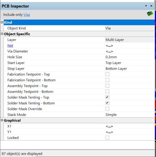
    Hopefully, someone with more experience using CS rules can help.  I know you can select the vias you want to tent and do them individually or as a group with PCB Inspector.  There is also a rules wizard that helps define rules but it doesn't allow you to add all the rules conditions that AD does.  Therefore, you cannot add the IsVia keyword or InNet or others I sort of remember from my AD days.


    However, if you know the rule keywords, or if you look them up in the AD documentation, you can export the rules from CS and edit them in a text editor and then import them back into CS and they should work.  Yes, this is a workaround and worthy perhaps of a verbal curse.


    By the way, your screen shot shows vias in pads and some vias much too close to pads.  You could fill and plate the vias or you should move them away further from the pads.  I'm used to hearing this covering referred to as solder mask (not silk mask).

    • Cancel
    • Vote Up 0 Vote Down
    • Cancel
  • lainscough_dfc
    lainscough_dfc over 5 years ago in reply to tarribred61

    In Designer, you do a SolderMaskExpansion Rule

    Select the via and set the expansion to 0 from Hole edge. Or thats the way I do it. Not quite sure what tenting is, still investigating that in Altium Designer at work.

    i.e

    image


    Not sure how you do the same in CS. There's a lot to learn on CS in terms of the way you do stuff, but getting quite impressed with the tool, so far. Docs are just a bit limited to find answer, but this forum works well.


    Can you elaborate on the PCB Inspector option a bit please, maybe pictures. Thanks


    I'm fine with a work around, so I will play with the import and export feature soon. Thanks


    I'm guilty of placing via's near to pad as close as I can as I like to keep the impedance down to the planes and use quite large tracks to help. Not heard it being a bad idea before, so open to know why. I try not to put via's in the pads, just to the side.


    Yes solder mask, not silk mask.

    • Cancel
    • Vote Up 0 Vote Down
    • Cancel
  • tarribred61
    tarribred61 over 5 years ago in reply to lainscough_dfc

    If you have access to AD then you should be able to export your rule from it into a text file and then import into CS.  I have not tried this recently but did it about a year ago from one of my old rules.

    To me, these vias are basically in the pads.  The via hole can steal solder off the pad and the joint may suffer.  But if it has worked for you then good luck.  My preference would be to use a short wide track covered with solder mask, much like a BGA pad to via dog-bone, or just extend the pad with a track that is the same width and covered with solder mask so solder won't pull off the pad and into the via.

    image

    • Cancel
    • Vote Up 0 Vote Down
    • Cancel
  • lainscough_dfc
    lainscough_dfc over 5 years ago in reply to lainscough_dfc

    I tried the Rule method but it would not except Via as an option Assuming you meant from the Rules edit and RHC export, import rule. No Luck.


    I then tried the Object Inspector method and yes it worked. Thanks


    The method for others to learn:-


    So Select only via with Home->Via.

    Drag around the entire board to select all via's.


    View->Object Inspector and select the tenting options. Says Only Via's at the top.

    image

    Close window.

    Generate the Gerbers.


    And in Gerbview (Kicad gerber viewer) has no Vias on the anti-solder mask layer.

    image


    Thanks, much appreciated.

    Lee

    • Cancel
    • Vote Up 0 Vote Down
    • Cancel
element14 Community

element14 is the first online community specifically for engineers. Connect with your peers and get expert answers to your questions.

  • Members
  • Learn
  • Technologies
  • Challenges & Projects
  • Products
  • Store
  • About Us
  • Feedback & Support
  • FAQs
  • Terms of Use
  • Privacy Policy
  • Legal and Copyright Notices
  • Sitemap
  • Cookies

An Avnet Company © 2026 Premier Farnell Limited. All Rights Reserved.

Premier Farnell Ltd, registered in England and Wales (no 00876412), registered office: Farnell House, Forge Lane, Leeds LS12 2NE.

ICP 备案号 10220084.

Follow element14

  • X
  • Facebook
  • linkedin
  • YouTube